
1 - 10 of 95
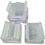
12 inch silicon wafer
Selling leads
|
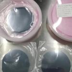
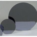
Product Description: Fused Silica Wafer is an optical-grade monocrystalline wafer made of quartz material, also known as fused quartz or fused silica. ...
2024-12-09 22:58:07
|
|
... of people. Silicon comes second as the most common element in the universe; it is mostly used as a semiconductor in the technology and electronic ...
2024-12-09 21:18:07
|
|
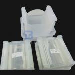
12 inch Silicon Wafer Prime Test Dummy Wafers Silicon wafer is a material used for producing semiconductors, which can be found in all types of ...
2024-12-09 21:18:07
|
|
... ingots to wafer processing. We have established the supply system mainly for the mass-produced wafers for bipolar integrated circuits, discrete ...
2024-12-09 20:34:25
|
|
...an ideal material for Anodic bonding. BonTek provides borosilicate wafers from 2 to 14 inches diameter, the thickness is 100um up with low ...
2024-12-09 20:34:25
|
|
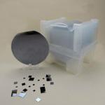
...Silicon Wafer With High Resistivity For Semiconductor Silicon wafers are thin slices of pure crystalized silicon. These pure forms of wafers are ...
2024-12-09 20:34:25
|
|
... electronics. BonTek offers Prime, Test, Monitor, SEMI standard, and customized silicon wafers in all diameters from 2″ to 300mm. Our silicon ...
2024-12-09 20:34:25
|
|
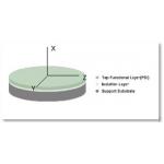
...r specific requirements are met by choosing prime grade and defecting free silicon wafer as a substrate so that a high uniform layer of thermal ...
2025-07-26 00:13:55
|
|
.... LNOI substrates are fabricated by transferring a thin layer of lithium niobate (LiNbO3) crystal onto an insulating substrate, typically silicon ...
2025-07-26 00:13:55
|

|
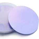
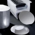
8 Inch 12 Inch Fused Quartz JGS1 Wafers For Optics Lasers And Semiconductors Fused Quartz JGS1 Features Fused quartz JGS1 is a high-quality synthetic ...
2025-07-26 00:13:55
|