Product Description:
Fused Silica Wafer is an optical-grade monocrystalline wafer made
of quartz material, also known as fused quartz or fused silica. It
has excellent optical properties, such as transmission range from
0.17 to 2.1um, 0.26 to 2.1um and 0.0185 to 3.5um, warp less than
35um, FLH Models such as JGS1, JGS2, JGS3 and F-HUV, second flat
per request, and surface roughness Ra less than 1.0nm. In
comparison with other materials such as calcium silicate board and
borosilicate glass, it has higher optical transmission, less
thermal expansion coefficient, and better homogeneity. Fused Silica
Wafer is the ideal material for high-precision optical components,
such as lenses, windows, and prisms.
Features:
- Product Name: Fused Silica Wafer
- Transmission: IR, Visible, DUV
- Metal Impurities: <0.2ppm
- BOW: <30um
- TTV: <2um, <5um
- Material: Fused Silica Glass
- Glass Wafer
- Fused Quartz Labware
- Aluminum Silicate Glass
- Optical Glass
Technical Parameters:
| Material | UV Fused Silica, Fused Quartz (JGS1, JGS2, JGS3) |
| Specification | unit | 3” | 4” | 5" | 6" | 8" | 12" |
| Diameter (or Square) | mm | 76.2 | 100 | 125 | 150 | 200 | 300 |
| Tol(±) | mm | <0.1~0.25 mm |
| Thinnest Thickness | mm | >0.10 | >0.10 | >0.30 | >0.30 | >0.30 | >0.50 |
| Primary Flat | mm | 22 | 32.5 | 42.5 | 57.5/notch | notch | notch |
| LTV (5mmx5mm) | µm | <2 | <2 | <2 | <2 | <2 | <10 |
| TTV | µm | <8 | <10 | <15 | <20 | <30 | <30 |
| Bow | µm | ±20 | ±25 | ±40 | ±40 | ±60 | ±60 |
| Warp | µm | <30 | <40 | <50 | <50 | <60 | <60 |
| PLTV(<0.5um) | % | ≥95%(5mm*5mm) |
| Transmittance | | UV, Optical, IR or Custom option |
| Edge Rounding | mm | Compliant with SEMI M1.2 Standard/refer to IEC62276 |
| Surface Type | | Single Side Polished /Double Sides Polished |
| Polished side Ra | nm | <1.0nm or specific per requested |
| Back Side Criteria | µm | General is 0.2-0.5µm or as customized |
| Appearance | Contamination | None |
| Particles>0.3µm | <=30 |
| Saw Marks, striations | None |
| Scratch | None |
| Cracks, saw marks, stains | None |
| Parameters | Specifications |
|---|
| Parallelism | 3 Arc Sec |
| Warp | <35um |
| Transmission | IR, Visible, DUV |
| Density | 2.20g/cm3 |
| Certificate | ISO9001, RoHS |
| OH Content | <5ppm, <10ppm, <100ppm |
| Damage Threshold | >10J/cm2 |
| FLH Model | JGS1, JGS2, JGS3, F-HUV |
| Thickness | 0.1-10mm |
| Surface Quality | 20-10 |
| Fused Quartz Labware | High Purity Fused Silica |
| Aluminum Silicate Glass | Yes |
Applications:
BonTek's high purity fused silica wafers are a type of glass
substrates made of calcium silicate board material with an
extremely low metal impurity level of less than 0.2ppm. These
wafers have a refractive index of 1.46, 1.472, 1.50, 1.51, 1.523
and a damage threshold of more than 10J/cm2. They are manufactured
according to ISO:9001 standards and beveled with 0.25mm X 45°
angle. Available in a variety of diameters ranging from 2 to 12
inches, BonTek's fused silica wafers are suitable for a wide range
of applications and offer outstanding durability and performance.
With a minimum order quantity of 5 pcs and a delivery time of 2
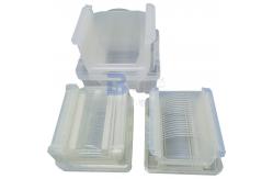
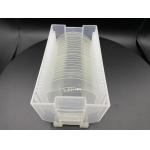
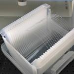
weeks, these wafers can be packaged in either a cassette or a jar
and are supplied in quantities of up to 100000 per month. The
alumina silicate glass used in the making of these wafers ensures
superior strength and heat resistance, making them the perfect
choice for any application requiring superior performance.
Customization:
Fused Silica Wafer
- Brand Name: BonTek
- Model Number: Glass substrates
- Place of Origin: China
- Certification: ISO:9001
- Minimum Order Quantity: 5 pcs
- Packaging Details: Cassette, Jar
- Delivery Time: 2 weeks
- Payment Terms: TT/in advance
- Supply Ability: 100000/month
- Diameter: 2-12 Inch
- Refractive Index: 1.46, 1.472, 1.50, 1.51, 1.523
- Transmission Range: 0.17~2.1um, 0.26~2.1um, .0185~3.5um
- Warp: <35um
- FLH Model: JGS1, JGS2, JGS3, F-HUV
- Keywords: Calcium Silicate Board, alumina silicate glass, Calcium Silicate
Board, high-temperature insulation material
Support and Services:
Fused Silica Wafer Technical Support and Service
We provide technical support and service for Fused Silica Wafer.
Our experienced technicians and engineers can provide the following
services:
- Repair and maintenance of Fused Silica Wafer products
- Consulting and troubleshooting of Fused Silica Wafer issues
- Installation and configuration of Fused Silica Wafer
- Testing and evaluation of Fused Silica Wafer
- Software upgrades for Fused Silica Wafer
- Training and support for Fused Silica Wafer
If you have any questions or need support for your Fused Silica
Wafer, please contact us for more information.