
91 - 98 of 98
semiconductor wafer processing laser equipment
Selling leads

|
...reaction-bonded silicon carbide (RBSiC) process. It is primarily designed for carrying and transporting wafers in high-temperature process ...
2025-10-29 12:53:17
|

|
...semiconductor manufacturing and precision optical equipment, such as lithography machines. It typically serves as the key sensor substrate within ...
2025-10-29 12:53:14
|

|
Product Description: VIS-NIR Camera CCD Contour-IR Contour-M Digital Camera 400-1700nm Multispectral Camera CONTOUR-IR near-infrared cameras are ...
2025-06-18 18:29:22
|

|
...Flip-Chip Bonding processes in semiconductor manufacturing. Its core function is to stably adsorb and secure wafers or dies during bonding, ...
2025-10-29 12:53:18
|
|
...- Research Dummy Grade SIC Epitaxial Substrates Features of SIC Wafers: Wide-band gap silicon carbide semiconductors are used to control and switch ...
2026-04-30 00:07:55
|

|
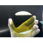
... (SiO₂), offering exceptional optical performance, thermal stability, and chemical resistance. They are widely used in laser technology, semiconduc...
2025-07-04 17:08:52
|

|
Product Description Sapphire Crystal Growth Furnace CZ method Czochralski Furnace produces high quality sapphire crystals ZMSH's CZ Puller furnaces ...
2025-06-18 18:29:21
|

|
... exceptional optical clarity, thermal stability, and chemical resistance. Designed for advanced optical systems, photonics, semiconductor ...
2026-04-30 00:07:55
|