
141 - 150 of 215
ssp semiconductor substrate
Selling leads
|
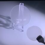
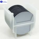
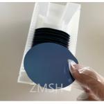
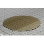
... Sapphire Wafers Crystal Substrates The specifications of 2inch sapphire wafer substrate Material: High Purity >99.99%, single crystal Al2O3 ...
2025-07-30 00:08:00
|
|
... as the foundation for high-performance semiconductor devices. Crafted with advanced float-zone mono-crystalline silicon technology, this substrate ...
2025-05-06 20:45:11
|
|
...substrates template,GaN wafer for LeD,semiconducting Gallium Nitride Wafer for ld,GaN template, mocvd GaN Wafer,Free-standing GaN Substrates by ...
2025-05-06 20:44:30
|
|
... substrate sapphire window sapphire wafer Applications of AlN template Silicon-based semiconductor technology has reached its limits and could not ...
2025-05-06 20:44:39
|
|
...Substrate 111 P Type N Type for Micro-electromechanical systems (MEMS) Or Power semiconductor devices Or Optical components and sensors Product ...
2025-05-06 20:45:50
|
|
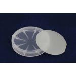
.... Featuring a thickness ranging from 10μm to 25μm, this crucial substrate is available in 6-inch and 8-inch diameters, ensuring versatility for ...
2025-05-06 20:45:05
|
|
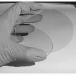
... for semiconductor devices. Their exceptional electrical conductivity properties, which can be precisely modified through doping with elements like ...
2025-05-06 20:45:58
|
|
... stations powering 5G networks, and integrated into tools manufacturing next-gen microchips, quartz wafers are essential. These high-purity ...
2025-07-10 18:23:13
|
|
dia50.8mm 2inch 1inch AlN substrate/AlN single crystal wafers 10x10mm or diameter 10mm dia25.4mm dia30mm, dia45mm, dia50.8mm AlN substrate AlN single ...
2025-05-06 20:44:42
|
|
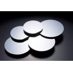
2inch /3inch 4inch /5inch C-axis/ a-axis/ r-axis/ m-axis 6"/6inch dia150mm C-plane Sapphire SSP/DSP wafers with 650um/1000um Thickness TTV
2025-05-06 20:38:48
|