
111 - 120 of 215
ssp semiconductor substrate
Selling leads
|
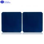
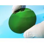
...Substrate Silicon carbide subatrte 4H/6H-P 3C-N 5×5 10×10mm P grade R grade D grade 4H/6H-P SiC Substrate 5×5 10×10mm's abstratct The 4H/6H-P ...
2025-05-06 20:41:41
|
|
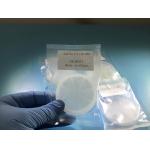
Product Description: Our InP (Indium Phosphide) semiconductor wafers, renowned for their exceptional electronic and optoelectronic properties, have ...
2025-05-06 20:44:23
|
|
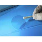
Ultra-thin 2inch sapphire DSP wafers thickness 100um 0.1mm 2inch 100um Ultra Thin sapphire wafers 0.1mm Thickness C-plane DSP Sapphire wafer Why ...
2025-05-06 20:38:59
|
|
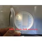
...substrates template,GaN wafer for LeD, semiconducting Gallium Nitride Wafer for ld, GaN template, mocvd GaN Wafer,Free-standing GaN Substrates by ...
2025-05-06 20:44:15
|
|
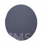
...substrates wafers/4 inch 4h-N type SIC Substrates 0.35 mm DSP Prime Zero Grade Silicon Carbide Wafer About Silicon Carbide (SiC)Crystal Silicon ...
2025-07-24 00:12:37
|
|
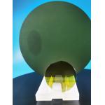
...Substrate DSP (111) Semiconductor RF Microwave LED Lasers Description of SiC Wafer: The 6-inch P-Type Silicon Carbide (SiC) Wafer in either 4H or ...
2025-05-06 20:41:42
|
|
...substrates AlN Wafer Characteristic III-Nitride(GaN,AlN,InN) 2inch AlN template on sapphire or sic substrates, HVPE Gallium Nitride wafer,AlN ...
2025-05-06 20:44:29
|
|
...Substrate/Wafers (150mm, 200mm) Silicon Carbide Ceramic Excellent CorrosionSingle crystal single side polished silicon wafer sic wafer polishing ...
2025-05-06 20:41:07
|
|
4inch 6inch 300-900 nm Lithium Niobate LiNbO3 LN Thin Films (LNOI) on silicon wafer Direction of application: · Electro-Optic Modulators · Delay Lines ...
2025-05-06 20:44:42
|
|
...substrates template,GaN wafer for LeD,semiconducting Gallium Nitride Wafer for ld,GaN template, mocvd GaN Wafer,Free-standing GaN Substrates by ...
2025-05-06 20:44:29
|