
131 - 140 of 261
single crystal silicon wafer substrate
Selling leads
|
...substrates wafers for GaN epitaxial growth;0.1mm/100um 2inch sapphire c-axis substrates 2Inch 3inch 4inch 0.43mm 0.1mm ultrathin thickness double ...
2025-05-06 20:38:50
|
|
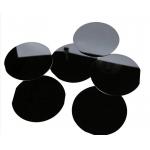
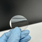
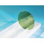
... with notch SSP DSP 1.0mm C - Axis sapphire optical glass windows PRODUCT SPECIFICATION Material: Single crystal Al2O3 99.999% Diameter:300.00±0...
2025-05-06 20:39:15
|
|
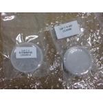
2inch InP wafers 3inch 4inch N/P TYPE InP Semiconductor Substrate Wafers Doped S+/ Zn+ /Fe + growth (modified VFG method) is used to pull a single ...
2025-05-06 20:44:37
|
|
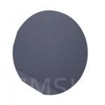
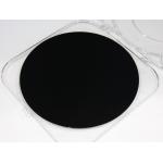
...leading manufacturer and supplier of SiC (Silicon Carbide) substrate wafer, ZMSH offers the best price on the market for 2 inch and 3 inch Research ...
2025-07-23 00:09:03
|
|
... Substrates. It has a crystal structure of silicon carbide where the silicon and carbon atoms are arranged in a cubic lattice with a diamond-like ...
2025-05-06 20:41:43
|
|
...wafer 1-5um AlN template 8inch 6inch AlGaN/GaN HEMT-on-HR Si Epiwafer GaN-on-Si Epiwafer for Micro-LED for RF application GaN Wafer Characteristic ...
2025-05-06 20:44:19
|
|
... on the market for 2 inch and 3 inch Research grade SiC substrate wafers. SiC substrate wafers have a variety of applications in electronic device ...
2025-07-23 00:09:03
|
|
...Substrate wafer Double Side Polished M Axis C Axis A Axis Special Orientation SSP/ DSP A-axis R-axis M-axis 2inch 3inch 4inch 6inch sapphire ...
2025-05-06 20:39:26
|
|
... resistant Highly chemical resistant Maximum temperature rating of almost 2000C The Detail for 2inch C-axis wafers Size: 2 inch DSP-0.1-C-Sapphire ...
2025-05-06 20:38:38
|
|
... Wafer Characteristic III-Nitride(GaN,AlN,InN) Gallium Nitride is one kind of wide-gap compound semiconductors. Gallium Nitride (GaN) substrate is ...
2025-05-06 20:44:18
|