
111 - 120 of 261
single crystal silicon wafer substrate
Selling leads
|
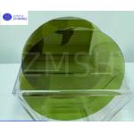
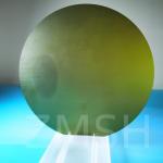
... carbon chips for optical About Silicon Carbide (SiC)Crystal Silicon carbide (SiC), also known as carborundum, is a semiconductor containing ...
2025-05-06 20:40:52
|
|
... optical lens for intermediate infrared laser Nonlinear optical and quantum optics lens About Silicon Carbide (SiC)Crystal Silicon carbide (SiC), ...
2025-05-06 20:40:53
|
|
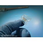
..., optoelectronic devices, semiconductor devices, and other fields. The high light transmittance and high hardness of sapphire wafers make them ...
2025-07-23 00:09:03
|
|
...: The ion implantation machine is used to drive high-energy He ions from the upper surface of lithium niobate crystal. When He ions with specific ...
2025-05-06 20:44:59
|
|
...Silicon LiNbO3 Lithium Niobate Wafer Thin Films Layer On Silicon Substrate Lithium niobate (LiNbO3) crystal is an important photoelectric material, ...
2025-05-06 20:44:57
|
|
dia50.8mm 2inch 1inch AlN substrate/AlN single crystal wafers 10x10mm or diameter 10mm dia25.4mm dia30mm, dia45mm, dia50.8mm AlN substrate AlN single ...
2025-05-06 20:44:42
|
|
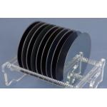
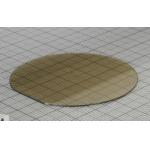
... to a silicon carbide (SiC) wafer with a 12-inch diameter (approximately 300mm), a size standard used in the semiconductor industry for the mass ...
2025-05-06 20:41:54
|
|
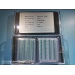
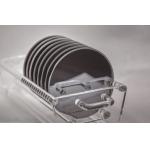
...Single Wafer Carrier, Single Wafer Sample Box for Silicon, Sapphire, SiC Substrate Cleanroom Class 100 Grade 1 inch Style Single Wafer Carrier ...
2025-05-06 20:47:34
|
|
...Wafer Thickness 600±50μm Customization Silicon carbide growth Description of SiC Seed Wafer: SiC seed crystal is actually a small crystal with the ...
2025-05-06 20:41:47
|
|
...Miscut A 4 Degree Sapphire Wafers Thickness 0.175mm/0.3mm/0.4mm/0.5mm Dsp 2 Inch C Plane Polished Sapphire Wafers Crystal Substrates The specificat...
2025-07-23 00:09:03
|