
71 - 80 of 129
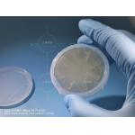
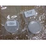
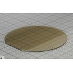
single crystal indium phosphide wafer
Selling leads
|
...Wafer 330um dummy research grade Customzied size/10x10x0.5mmt/2inch/3inch/4inch/6inch 6H-N/4H-SEMI/ 4H-N SIC ingots/High purity 4H-N 4inch 6inch ...
2025-05-06 20:40:51
|
|
... dia 150mm silicon carbide single crystal (sic) substrates wafersS/ High purity un-doped 4H-semi resistivity>1E7 3inch 4inch 0.35mm sic wafers ...
2025-05-06 20:40:51
|
|
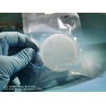
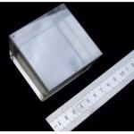
...Wafer Si Substrate 111 P Type N Type for Micro-electromechanical systems (MEMS) Or Power semiconductor devices Or Optical components and sensors ...
2025-05-06 20:45:50
|
|
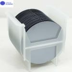
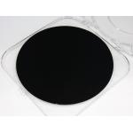
High Purity 4 6 8-inch conductive semi insulation SiC single crystal wafer/8 Inches (200mm) Monocrystalline Double Side Polished SiC Wafer/Silicon ...
2025-05-06 20:41:06
|
|
...wafer 1-5um AlN template 8inch 6inch AlGaN/GaN HEMT-on-HR Si Epiwafer GaN-on-Si Epiwafer for Micro-LED for RF application GaN Wafer Characteristic ...
2025-05-06 20:44:19
|
|
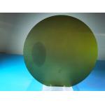
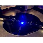
...crystals crystal substrate TeO2 wafer TeO2 Crystal & Q Switch TeO2 is an excellent ascousto-optic (AO) crystal with high AO figure of merit, ...
2025-05-06 20:40:28
|
|
... Wafer Characteristic III-Nitride(GaN,AlN,InN) Gallium Nitride is one kind of wide-gap compound semiconductors. Gallium Nitride (GaN) substrate is ...
2025-05-06 20:44:18
|
|
... Wafer Characteristic III-Nitride(GaN,AlN,InN) Gallium Nitride is one kind of wide-gap compound semiconductors. Gallium Nitride (GaN) substrate is ...
2025-05-06 20:44:18
|
|
dia50.8mm 2inch 1inch AlN substrate/AlN single crystal wafers 10x10mm or diameter 10mm dia25.4mm dia30mm, dia45mm, dia50.8mm AlN substrate AlN single ...
2025-05-06 20:44:42
|
|
..., optoelectronic devices, semiconductor devices, and other fields. The high light transmittance and high hardness of sapphire wafers make them ...
2025-07-25 00:10:23
|