
11 - 20 of 172
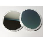
semiconductor inas substrate
Selling leads
|
...film on silicon substrate Applications of AlN template Silicon-based semiconductor technology has reached its limits and could not satisfy the ...
2025-05-06 20:44:41
|
|
...AlN substrate AlN single crystal wafers Applications of AlN template Silicon-based semiconductor technology has reached its limits and could not ...
2025-05-06 20:44:41
|
|
...variety of applications in the telecommunications, optoelectronics, and semiconductor industries. With superior optical and electronic properties, ...
2025-05-06 20:45:10
|
|
...Wafer with (111) Crystal Orientation – Introduction The 8-inch silicon wafer with (111) crystal orientation is a vital component in the semiconduct...
2025-05-06 20:45:52
|
|
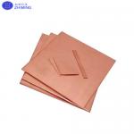
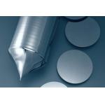
...substrate single crystal Cu wafer 5x5x0.5/lmm 10x10x0.5/1mm 20x20x0.5/1mm a=3.607A Copper substrate's abstract Our copper substrates and wafers are ...
2025-05-06 20:45:45
|
|
... GaAs Wafer Product Description (GaAs) Gallium Arsenide Wafers PWAM Develops and manufactures compound semiconductor substrates-gallium arsenide ...
2025-05-06 20:44:31
|
|
2inch InP wafers 3inch 4inch N/P TYPE InP Semiconductor Substrate Wafers Doped S+/ Zn+ /Fe + growth (modified VFG method) is used to pull a single ...
2025-05-06 20:44:36
|
|
2inch InP wafers 3inch 4inch N/P TYPE InP Semiconductor Substrate Wafers Doped S+/ Zn+ /Fe + growth (modified VFG method) is used to pull a single ...
2025-05-06 20:44:37
|
|
...film on silicon substrate Applications of AlN template Silicon-based semiconductor technology has reached its limits and could not satisfy the ...
2025-05-06 20:44:40
|
|
...substrate Ge window for infrared Co2 lasers Ge Material Introduce Among optical materials, germanium materials are increasingly widely used in ...
2025-05-06 20:44:48
|