
11 - 20 of 286
sapphire semiconductor substrate
Selling leads
|
...Semiconductor Substrate For Epitaxial Growth VGF 2inch 4inch 6inch n-type prime grade GaAs wafer for epitaxial growth Gallium arsenide can be made ...
2025-05-06 20:45:00
|
|
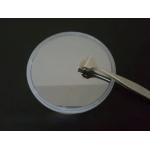
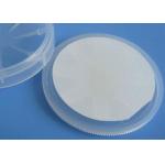
Ultra-thin 2inch sapphire DSP wafers thickness 100um 0.1mm Why Sapphire? One of the hardest materials available Superior IR & UV transmission compared ...
2025-05-06 20:38:38
|
|
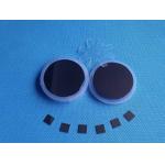
... GaAs Wafer Product Description (GaAs) Gallium Arsenide Wafers PWAM Develops and manufactures compound semiconductor substrates-gallium arsenide ...
2025-05-06 20:44:31
|
|
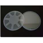
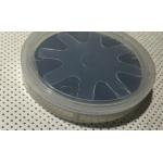
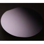
2inch InP wafers 3inch 4inch N/P TYPE InP Semiconductor Substrate Wafers Doped S+/ Zn+ /Fe + growth (modified VFG method) is used to pull a single ...
2025-05-06 20:44:36
|
|
2inch InP wafers 3inch 4inch N/P TYPE InP Semiconductor Substrate Wafers Doped S+/ Zn+ /Fe + growth (modified VFG method) is used to pull a single ...
2025-05-06 20:44:37
|
|
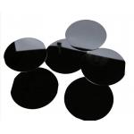
...substrate, and an infrared light-emitting device with a wavelength of 2 to 14 μm can be fabricated. The AlGaSb superlattice structure material can ...
2025-05-06 20:44:36
|
|
...substrates template,GaN wafer for LeD,semiconducting Gallium Nitride Wafer for ld,GaN template, mocvd GaN Wafer,Free-standing GaN Substrates by ...
2025-05-06 20:44:29
|
|
... on silicon substrate Applications of AlN template Silicon-based semiconductor technology has reached its limits and could not satisfy the ...
2025-05-06 20:44:38
|
|
...film on silicon substrate Applications of AlN template Silicon-based semiconductor technology has reached its limits and could not satisfy the ...
2025-05-06 20:44:41
|
|
...AlN substrate AlN single crystal wafers Applications of AlN template Silicon-based semiconductor technology has reached its limits and could not ...
2025-05-06 20:44:41
|