
51 - 60 of 286
sapphire semiconductor substrate
Selling leads
|
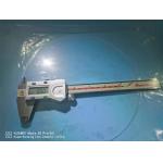
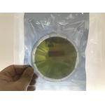
...Sapphire Wafers For epitaxial Thickness 500um Double side polished DSP Special Orientation SSP/ DSP A-axis R-axis M-axis 2inch 3inch 4inch 6inch ...
2025-05-06 20:38:51
|
|
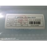
...Sapphire Wafers Thickness 500UM 600um Double side polished SSP OR DSP Special Orientation SSP/ DSP A-axis R-axis M-axis 2inch 3inch 4inch 6inch ...
2025-05-06 20:38:51
|
|
Product Overview TGV (Through Glass Via) technology, also known as glass through-hole technology, is a vertical electrical interconnection technique ...
2025-07-30 00:08:00
|
|
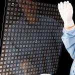
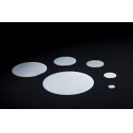
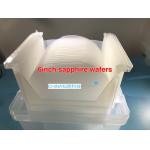
... diameter 300mm with notch DSP Sapphire Substrate wafers thickness 1.5mm C-a Diameter 156mm 200mm 8inch double side polished Sapphire Substrate for ...
2025-05-06 20:38:54
|
|
... FOR PART ORIENTATION: Why Sapphire? Chemical resistance – sapphire is highly inert and resistant to attack in most process environments.Mechanical ...
2025-05-06 20:38:54
|
|
...Material Sapphire(Al2O3) Density(20°C) Kg/M3 3.98×10³ Crystal Structure Hexagonal Crystal Lattice Constant A=4.785Å C=12....
2025-05-06 20:39:16
|
|
...> M-axis 2inch 3inch 4inch 6inch sapphire substrates wafers for GaN epitaxial growth;0.1mm/100um 2inch sapphire c-axis substrates TYPICAL CHOICES ...
2025-05-06 20:38:43
|
|
...supplier of sapphire substrates for photoelectronic applications, including the high brightness LED market. The material is grown and orientated, ...
2025-07-30 00:08:00
|
|
...substrates wafers, sic crystal ingots sic semiconductor substrates,Silicon Carbide crystal Wafer/ Customzied as-cut sic wafers About Silicon ...
2025-05-06 20:40:37
|
|
...) and 5500 nm (IR) (the visible spectrum extends about 380 nm to 750 nm, and extraordinarily scratch-resistant. The key benefits of sapphire ...
2025-05-06 20:40:24
|