
51 - 60 of 151
polypropylene single wafer box
Selling leads
|
...wafer 1mm thickness for ingot growth Customzied size/2inch/3inch/4inch/6inch 6H-N/4H-SEMI/ 4H-N SIC ingots/High purity 4H-N 4inch 6inch dia 150mm ...
2025-05-06 20:40:54
|
|
... Wafer Characteristic III-Nitride(GaN,AlN,InN) Gallium Nitride is one kind of wide-gap compound semiconductors. Gallium Nitride (GaN) substrate is ...
2025-05-06 20:44:18
|
|
... Wafer Characteristic III-Nitride(GaN,AlN,InN) Gallium Nitride is one kind of wide-gap compound semiconductors. Gallium Nitride (GaN) substrate is ...
2025-05-06 20:44:18
|
|
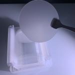
...Seed Wafer Thickness 600±50μm Customization Silicon carbide growth Description of SiC Seed Wafer: SiC seed crystal is actually a small crystal with ...
2025-05-06 20:41:47
|
|
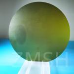
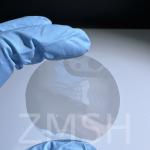
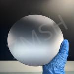
..., optoelectronic devices, semiconductor devices, and other fields. The high light transmittance and high hardness of sapphire wafers make them ...
2025-07-30 00:08:00
|
|
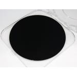
4H N Type Semi Type SiC Wafer 4inch DSP Production Research Dummy Grade Customization *, *::before, *::after {box-sizing: border-box;}* {margin: 0;...
2025-05-06 20:41:26
|
|
2inch Silicon Carbide wafer Diameter 50.8mm P grade R grade D drade Double Side Polished *, *::before, *::after {box-sizing: border-box;}* {margin: 0;...
2025-05-06 20:41:27
|
|
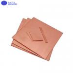
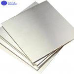
...single crystal Cu wafer 5x5x0.5/lmm 10x10x0.5/1mm 20x20x0.5/1mm a=3.607A Copper substrate's abstract Our copper substrates and wafers are made from ...
2025-05-06 20:45:45
|
|
...advanced materials research and applications due to their unique physical properties, such as lightweight and excellent thermal conductivity. These ...
2025-05-06 20:45:46
|
|
... conductivity properties, which can be precisely modified through doping with elements like phosphorus or boron, make them ideal for fabricating ...
2025-05-06 20:45:58
|