
271 - 280 of 311
inp semiconductor substrate wafers
Selling leads
|
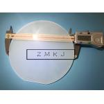
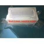
2inch /3inch 4inch /5inch C-axis/ a-axis/ r-axis/ m-axis 6"/6inch dia150mm C-plane Sapphire SSP/DSP wafers with 650um/1000um Thickness About synthetic ...
2025-05-06 20:38:39
|
|
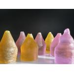
10x10mmt Terbium gallium garnet (TGG)crystals substrate wafer for laser device Product Type: Yttrium aluminum garnet (YAG) is an isotropic crystal ...
2025-07-23 00:09:03
|
|
*, *::before, *::after {box-sizing: border-box;}* {margin: 0;}html, body {height: 100%;}body {line-height: 1.5;-webkit-font-smoothing: antialiased;...
2025-07-23 00:09:03
|
|
2inch /3inch 4inch /5inch C-axis/ a-axis/ r-axis/ m-axis 6"/6inch dia150mm C-plane Sapphire SSP/DSP wafers with 650um/1000um Thickness About synthetic ...
2025-05-06 20:38:43
|
|
2inch /3inch 4inch /5inch C-axis/ a-axis/ r-axis/ m-axis 6"/6inch dia150mm C-plane Sapphire SSP/DSP wafers with 650um/1000um Thickness About synthetic ...
2025-05-06 20:38:42
|
|
8inch/6inch/5inch/ 2inch /3inch 4inch /5inch C-axis/ a-axis/ r-axis/ m-axis 6"/6inch dia150mm C-plane Sapphire SSP/DSP wafers with 650um/1000um ...
2025-05-06 20:38:46
|
|
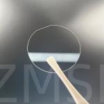
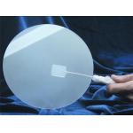
10*10*0.1mmt 100um 2inch sapphire wafers double side polished What is Sapphire orientation Zero Degree: The direction of view is parallel to the ...
2025-05-06 20:38:58
|
|
2inch 4inch 4" Sapphire based GaN templates GaN film on sapphire substrate Properties of GaN Chemical properties of GaN 1) At room temperature, GaN is ...
2025-05-06 20:39:23
|
|
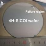
Introduce Silicon Carbide on Insulator (SiCOI) thin films are innovative composite materials, typically fabricated by depositing a single-crystal, ...
2025-05-27 17:33:30
|
|
..., GaN, and SiC. It plays an essential role in applications like power devices, MEMS, and CMOS image sensors. Working Principle The wafer thinning
2025-07-23 00:09:03
|