
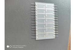
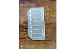
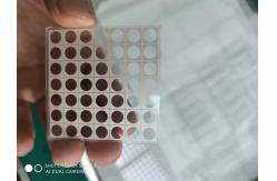
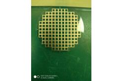
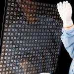
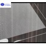
Sapphire Wafer With Metallization Circuit Board
|
|
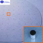
2inch 4inch 4" Sapphire based GaN templates GaN film on sapphire substrate
Properties of GaN Chemical properties of GaN1) At room temperature, GaN is insoluble in water, acid and alkali. 2)Dissolved in a hot alkaline solution at a very slow rate. 3) NaOH, H2SO4 and H3PO4 can quickly corrode the poor quality of GaN, can be used for these poor quality GaN crystal defect detection. 4) GaN in the HCL or hydrogen, at high temperature presents unstable characteristics. 5) GaN is the most stable under nitrogen. Electrical properties of GaN1) The electrical properties of GaN are the most important factors affecting the device. 2) The GaN with no doping was n in all the cases, and the electron concentration of the best sample was about 4*(10^16)/c㎡. 3) Generally, the prepared P samples are highly compensated. Optical properties of GaN1) Wide band gap compound semiconductor material with high band width (2.3~6.2eV), can cover the red yellow green, blue, violet and ultraviolet spectrum, so far is that any other semiconductor materials are unable to achieve. 2) Mainly used in blue and violet light emitting device. Properties of GaN Material1) High frequency property, arrive at 300G Hz. (Si is 10G & GaAs is 80G)2) High temperature property, Normal work at 300℃, very suitable for aerospace, military and other high temperature environment. 3) The electron drift has high saturation velocity, low dielectric constant and good thermal conductivity. 4) Acid and alkali resistance, corrosion resistance, can be used in harsh environment. 5) High voltage characteristics, impact resistance, high reliability. 6) Large power, the communication equipment is very eager. Application of GaN Main usage of GaN:1) light emitting diodes, LED 2) field effect transistors, FET 3) laser diodes, LD
Specification Caracteristic Specification
Other relaterd 4INCH GaN Template Specification
|
||||||||||||||||||||||||||||||||||||||||||||||||||||||||||||||||||||
| Product Tags: Sapphire Wafer Circuit Board Metallization Sapphire Wafer Sapphire Semiconductor Substrate | ||||||||||||||||||||||||||||||||||||||||||||||||||||||||||||||||||||
|
TGV Glass Substrate Through-hole Coating Semiconductor Packaging JGS1 JGS2 |
|
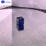
Royal Blue Sapphire Raw Gemstone Synthetic Colored For Durable Exquisite Jewelry & Watch Case |
|
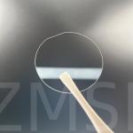
Sapphire Wafer Monocrystal Al2O3 DSP SSP 2inch 4inch 6inch 8inch 12inch A plane C plane |
|
Sapphire wafer 2inch C-plane(0001) DSP SSP 99,999% Monocrystalline Al2O3 LEDS Semiconductor |
|
Through Glass Vias (TGV) For JGS1 JGS2 Sapphire Corning Glass For Sensors Manufacturing And Packaging |
|
Through Glass Vias (TGV) JGS1 JGS2 Sapphire BF33 Quartz Customizable Dimensions Thickness Can Low As 100 Μm |