
261 - 270 of 311
inp semiconductor substrate wafers
Selling leads
|
...semiconductor wafers Excellent corrosion resistance. silicon carbide ceramic tray‘s short brief Silicon carbide (SiC) ceramic trays are specialized ...
2025-05-06 20:47:46
|
|
...wafers for High temperature superconducting junction technology Product Name:Strontium titanate (SrTiO 3) crystal substrateProduct Description: ...
2025-05-06 20:40:34
|
|
... wafer 4H N-Type CVD Orientation : 4.0°±0.5° Semi-Insulating 3-Inch Silicon Carbide wafer's Abstract The unique electronic and thermal properties ...
2025-05-06 20:41:19
|

|
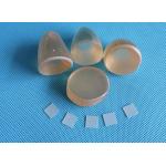
...Wafer Double Side Polished 2inch diameter TTV Bow Warp Product Description: There are many different polymorphs of silicon carbide and 6H silicon ...
2025-05-06 20:41:25
|
|
...second-generation semiconductor materials represented by silicon (Si) and gallium arsenide (GaAs) has propelled the swift advancement of microelect...
2025-05-06 20:41:29
|
|
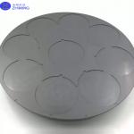
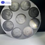
Introduction Of SIC Ceramic Tray SIC Ceramic Tray (Silicon Carbide Ceramic Tray) is a high-performance industrial carrier tool based on silicon ...
2025-06-23 17:13:00
|
|
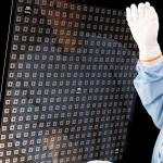
Product Overview TGV (Through Glass Via) technology, also known as glass through-hole technology, is a vertical electrical interconnection technique ...
2025-07-23 00:09:03
|
|
...Monocrystal KY Method LED Semiconductor 1. Abstract Our Sapphire Material 99.999% Al2O3 Monocrystal, produced using the KY (Kyropoulos) method, is ...
2025-05-06 20:40:05
|
|
... dia 150mm silicon carbide single crystal (sic) substrates wafersS/ Customzied as-cut sic wafers About Silicon Crystal * Low Dispersion and Density ...
2025-07-23 00:09:03
|
|
2inch /3inch 4inch /5inch C-axis/ a-axis/ r-axis/ m-axis 6"/6inch dia150mm C-plane Sapphire SSP/DSP wafers with 650um/1000um Thickness About synthetic ...
2025-05-06 20:38:40
|