
31 - 40 of 173
inp semiconductor substrate
Selling leads

|
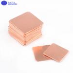
...substrate single crystal Aluminum substrate orientation 111 100 111 5×5×0.5mm a=4.040Ã single crystal Aluminum substrate's brief The demand for ...
2025-05-06 20:45:43
|
|
... to deliver optimal electrical and thermal performance for advanced semiconductor and electronic applications. These wafers are available in ...
2025-05-06 20:45:45
|
|
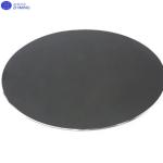
..., providing high-quality silicon carbide substrates that facilitate cutting-edge semiconductor research and development. 2. Product & Compony ...
2025-05-06 20:45:54
|
|
2-4inch Gallium antimonide GaSb Substrate Single Crystal Monocrystal for Semiconductor Gallium antimonide (GaSb) is a very important III-V direct ...
2025-05-06 20:44:35
|
|
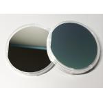
...Wafer with (111) Crystal Orientation – Introduction The 8-inch silicon wafer with (111) crystal orientation is a vital component in the semiconduct...
2025-05-06 20:45:52
|
|
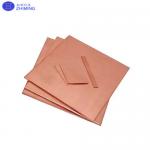
...substrate single crystal Cu wafer 5x5x0.5/lmm 10x10x0.5/1mm 20x20x0.5/1mm a=3.607A Copper substrate's abstract Our copper substrates and wafers are ...
2025-05-06 20:45:45
|
|
...film on silicon substrate Applications of AlN template Silicon-based semiconductor technology has reached its limits and could not satisfy the ...
2025-05-06 20:44:40
|
|
.... Silicon, a semiconductor material, is used to manufacture these wafers due to its excellent electrical properties. Silicon wafers are thin, disk...
2025-05-06 20:45:08
|
|
2inch 3inch 4inch InAs Wafer Crystal Substrates N-Type For MBE 99.9999% Monocrystalline Introduce of InAs substrate Indium InAs or indium mono...
2025-05-06 20:44:58
|
|
Al substrate single crystal Aluminum substrate purity 99/99% 5×5×1/0.5 mm 10×10×1/0.5 20x20x0.5/1mm Al substrate's abstract Single crystal aluminum ...
2025-05-06 20:45:42
|