
61 - 70 of 173
inp semiconductor substrate
Selling leads
|
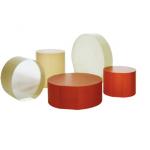
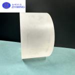
2inch/3inch/4inch/6inch Y-42°/36°/128° LT Lithium tantalate (LiTaO3) crystal / Fe+ doped type 250um/300um substrate wafer Product Name:Lithium ...
2025-05-06 20:44:34
|
|
2inch 3inch 4inch LNOI LiNbO3 Wafer Lithium Niobate Thin Films Layer On Silicon Substrate LNOI wafer preparation process is shown below, including the ...
2025-05-06 20:44:59
|
|
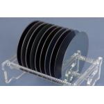
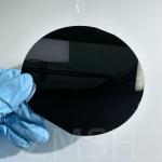
2inch 4inch LiTaO3 Wafer Substrate Double or Single Polished Z-cut X-cut Y-cut Saw grade Description of LiTaO3 Wafer: Lithium tantalate (LiTaO3) has a ...
2025-05-06 20:45:49
|
|
ZnTe Crystal Substrate Orientation110 10x10x0.5mm 10x10x1mm For THz Detection, THz Generation ZnTe crystals are excellent terahertz crystals lt;110> ...
2025-05-06 20:45:04
|
|
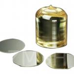
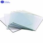
ITO Glass Substrate Indium Tin Oxide Coated Glass In2O3/SnO2 10 x 10 50×50 1.1mm thickness ITO Glass’s abstract ITO (Indium Tin Oxide) glass is a ...
2025-05-06 20:45:57
|
|
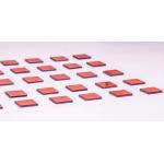
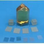
SrLaAlO₄ /LaSrAlO₄ LSAO10x10x0.5mmt5x5x1mmt Substrate for Epitaxy customized Abstract of SrLaAlO₄ / LaSrAlO₄/LASO SrLaAlO₄ , also written as LaSrAlO₄ ...
2025-05-27 17:33:28
|
|
...Substrates Wafer DSP Notch High Precision 8inch/6inch/5inch/ 2inch /3inch 4inch /5inch C-axis/ a-axis/ r-axis/ m-axis 6"/6inch dia150mm C-plane ...
2025-05-06 20:39:17
|
|
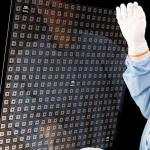
Product Overview TGV (Through Glass Via) technology, also known as glass through-hole technology, is a vertical electrical interconnection technique ...
2025-07-27 00:09:14
|
|
...Monocrystal KY Method LED Semiconductor 1. Abstract Our Sapphire Material 99.999% Al2O3 Monocrystal, produced using the KY (Kyropoulos) method, is ...
2025-05-06 20:40:05
|
|
Si wafer 4inch Polished CZ Dopant Arsenic(As) Boron(B) Phosphorus(Ph) (100) Semiconductor Describe of Si Wafer: A Silicon wafer is a very thin round ...
2025-05-06 20:45:29
|