
251 - 260 of 395
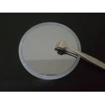
high transmittance sapphire substrate
Selling leads
|
...Substrate For Epitaxial Growth VGF 2inch 4inch 6inch n-type prime grade GaAs wafer for epitaxial growth Gallium arsenide can be made into semi...
2025-05-06 20:45:00
|
|
... (GaN) layer on a silicon (Si) substrate, which is 8 inches in diameter. This combination leverages GaN's high electron mobility, thermal ...
2025-05-06 20:45:22
|
|
...Substrate Single Crystal Monocrystal for Semiconductor Gallium antimonide (GaSb) is a very important III-V direct bandgap semiconductor material. ...
2025-05-06 20:44:35
|
|
...substrate Applications of AlN template Silicon-based semiconductor technology has reached its limits and could not satisfy the requirements of ...
2025-05-06 20:44:40
|
|
...substrate Applications of AlN template Silicon-based semiconductor technology has reached its limits and could not satisfy the requirements of ...
2025-05-06 20:44:41
|
|
...substrate AlN single crystal wafers Applications of AlN template Silicon-based semiconductor technology has reached its limits and could not ...
2025-05-06 20:44:41
|
|
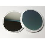
...t combines high optical transparency with excellent electrical conductivity. Typically composed of indium oxide (In₂O₃) doped with tin oxide (SnO₂)...
2025-05-06 20:45:57
|
|
|
... to 100mm Length from 2mm to 100mm Coating upon your request Ø Best materials for ultrashort pulse generation Ø Tunable range from 600-1100nm Ø ...
2025-05-13 05:29:53
|
|
|
... to 100mm Length from 2mm to 100mm Coating upon your request Ø Best materials for ultrashort pulse generation Ø Tunable range from 600-1100nm Ø ...
2025-05-13 05:29:56
|
|
...-state lasers (e.g. based on neodymium or ytterbium-doped gain media), since they can easily be tuned to the required pump wavelength and allow one ...
2025-07-29 00:07:53
|