
71 - 80 of 227
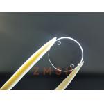
high optical transmittance sapphire substrate
Selling leads
|
...Sapphire The growth of superconducting compounds / Gallium Nitride Infrared detectors Hybrid microelectronics Polishing carriers Hostile environmen...
2025-05-06 20:37:41
|
|
...KY process) for sapphire crystal growth is currently used by many companies in China to produce sapphire for the electronics and optics industries. ...
2025-05-06 20:38:39
|
|
Sapphire wafer 8inch Diameter 200mm C Plane A Plane KY EFG Double Slide Polished Product Description: In 1992, Japanese engineer Shuji Nakamura ...
2025-05-06 20:39:56
|
|
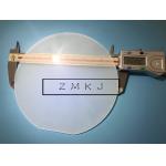
8inch/6inch/5inch/ 2inch /3inch 4inch /5inch C-axis/ a-axis/ r-axis/ m-axis 6"/6inch dia150mm C-plane Sapphire SSP/DSP wafers with 650um/1000um ...
2025-05-06 20:38:48
|
|
... inside an equipment or directly used for watching windows because of its very good physical property. For the physical characteristics of sapphire ...
2025-05-06 20:37:05
|
|
...Sapphire based GaN templates GaN film on sapphire substrate Properties of GaN Chemical properties of GaN 1) At room temperature, GaN is insoluble ...
2025-05-06 20:39:23
|
|
...making them highly desirable for a wide range of applications. In fact, sapphire is one of the hardest and most scratch-resistant materials ...
2025-07-27 00:09:14
|

|
...sapphire optical window monocrystalline Synthetic sapphire window Optical glass Window with step Sapphire application Application Sapphire wafer ...
2025-05-06 20:37:41
|

|
... quality for semiconductor applications. Known for its superior optical transparency, outstanding mechanical strength, and excellent thermal ...
2025-05-06 20:40:12
|
|
2inch 50.8mm C Miscut A 4 Degree Sapphire Wafers Thickness 0.175mm/0.3mm/0.4mm/0.5mm Dsp 2 Inch C Plane Polished Sapphire Wafers Crystal Substrates ...
2025-07-27 00:09:14
|