
221 - 227 of 227
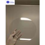
high optical transmittance sapphire substrate
Selling leads
|
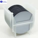
...Substrate 111 P Type N Type for Micro-electromechanical systems (MEMS) Or Power semiconductor devices Or Optical components and sensors Product ...
2025-05-06 20:45:50
|
|
... stations powering 5G networks, and integrated into tools manufacturing next-gen microchips, quartz wafers are essential. These high-purity ...
2025-07-10 18:23:13
|
|
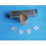
...substrate Product Description: Rutile (TiO2) large birefringence, large refractive index, is a method for spectral prism devices such as optical ...
2025-05-06 20:40:35
|
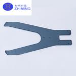
SiC Wafer Hand for Wafer Handling, Cleanroom Compatible, Corrosion Resistant, Customizable Interface
|
..., it offers excellent mechanical strength, corrosion resistance, thermal durability, and ultra-clean performance. It is ideal for handling advanced ...
2025-05-29 00:09:29
|
|
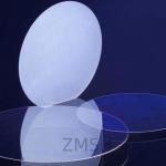
Fused Silica wafer JGS1 JGS2 BF33 8inch 12inch thickeness 750um±25um Ra ≤ 0.5nm TTV ≤ 10um Fused Silica wafer JGS1 JGS2 BF33 8inch 12inch‘s summary ...
2025-05-06 20:45:40
|
|
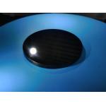
High Quality Silicon-on-Insulator Wafers SIC Silicon Carbide Wafers Customized High quality high precision Dia.700mm Sic spherical Mirror metal ...
2025-05-06 20:41:05
|
|
ZnTe: ZnTe wafer, ZnTe crystal Type N, Type P, Custom Sizes and Specifications Available Abstract of ZnTe Zinc telluride (ZnTe) is a direct bandgap ...
2025-05-06 20:45:56
|