
51 - 60 of 227
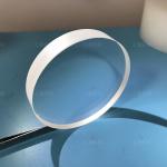
high optical transmittance sapphire substrate
Selling leads
|
...sapphire substrates wafers for GaN epitaxial growth;0.1mm/100um 2inch sapphire c-axis substrates TYPICAL CHOICES FOR PART ORIENTATION: Why Sapphire...
2025-05-06 20:39:19
|
|
...supplier of sapphire substrates for photoelectronic applications, including the high brightness LED market. The material is grown and orientated, ...
2025-07-27 00:09:14
|
|
...PART ORIENTATION: Why Sapphire? Zero Degree: The direction of view is parallel to the optical axis of the crystal 90 Degree: The direction of view ...
2025-05-06 20:38:55
|
|
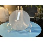
High Transmittance Infrared Sapphire Optical Windows Double Side Polished 60/40 Plano sapphire device viewing window by customized rectangle ...
2025-05-06 20:37:36
|
|
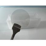
High Purity Substrate DSP/SSP Polished Sapphire Wafer Lens for sale Sapphire Optical Custom-made High Precision Transparent Sapphire Glass Optical ...
2025-05-06 20:38:05
|
|
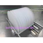
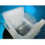
...Sapphire Window Substrates Wafer DSP Notch High Precision 8inch/6inch/5inch/ 2inch /3inch 4inch /5inch C-axis/ a-axis/ r-axis/ m-axis 6"/6inch ...
2025-05-06 20:39:17
|
|
...sapphire substrates wafers for GaN epitaxial growth; TYPICAL CHOICES FOR PART ORIENTATION: Why Sapphire? Zero Degree: The direction of view is ...
2025-05-06 20:38:38
|
|
... for 2inch, 4inch, 6inch sapphire substrates and sapphire windows. It is characterized by its extremely low surface roughness (Ra
2025-05-06 20:39:31
|
|
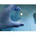
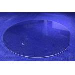
High transmittance 99% 1/4lambda flatness dia50/dia60/dia100mm sapphire optical lens Plano sapphire device viewing window by customized rectangle ...
2025-05-06 20:37:32
|
|
... The Kyropoulos process (KY process) for sapphire crystal growth is currently used by many companies in China to produce sapphire for the ...
2025-05-06 20:39:27
|