
121 - 130 of 203
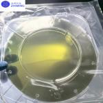
gallium oxide semiconductor substrate
Selling leads
|
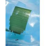
... For seed growth 6H-N/6H-Semi 4H HPSI 5*10mmt 10x10mmt 5*5mm polished Silicon Carbide sic substrate chips Wafer About Silicon Carbide (SiC)Crystal ...
2025-07-24 00:12:37
|
|
... (SiC) wafers and substrates are specialized materials used in semiconductor technology made from silicon carbide, a compound known for its high ...
2025-05-06 20:41:28
|
|
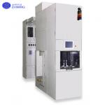
..., supports various oxidation, annealing, and LPCVD processes. The system features a 21-cassette automatic transfer with seamless MES integration, ...
2025-07-24 00:12:38
|
|
*, *::before, *::after {box-sizing: border-box;}* {margin: 0;}html, body {height: 100%;}body {line-height: 1.5;-webkit-font-smoothing: antialiased;...
2025-07-24 00:12:37
|
|
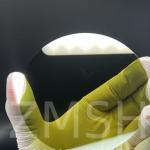
12inch SiC wafer Silicon Carbide wafer 300mm 750±25um 4H-N type orientation 100 Production Research grade 12inch SiC wafer's abstract This 12-inch ...
2025-05-06 20:41:55
|
|
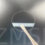
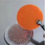
SiC Epitaxial Wafer Overview 4-inch (100 mm) SiC Epitaxial Wafers continue to play a vital role in the semiconductor market, serving as a highly ...
2025-07-10 18:23:23
|
|
...substrates template,GaN wafer for LeD,semiconducting Gallium Nitride Wafer for ld,GaN template, mocvd GaN Wafer,Free-standing GaN Substrates by ...
2025-05-06 20:44:12
|
|
...substrates template,GaN wafer for LeD,semiconducting Gallium Nitride Wafer for ld,GaN template, mocvd GaN Wafer,Free-standing GaN Substrates by ...
2025-05-06 20:44:28
|
|
...(GaN,AlN,InN) Gallium Nitride is one kind of wide-gap compound semiconductors. Gallium Nitride (GaN) substrate is a high-quality single-crystal ...
2025-05-06 20:44:18
|
|
...semiconductor substrate primarily used in the fabrication of various electronic and optoelectronic devices. Gallium Phosphide (GaP) wafers exhibit ...
2025-05-06 20:45:06
|