
131 - 140 of 203
gallium oxide semiconductor substrate
Selling leads
|
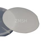
...wafers refers to a substrate material composed of a sapphire substrate with a layer of gallium nitride (GaN) grown on top. GaN is a semiconductor ...
2025-05-06 20:44:26
|

|
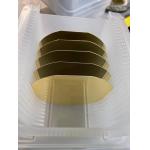
.../3 inch/4 inch 350-650 um InP Crystal Wafer Dummy Prime Semiconductor Substrate Shanghai Xinkehui New Materials Co. Ltd. We specialize in ...
2025-07-24 00:12:37
|
|
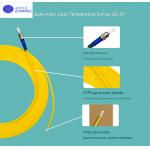
...Gallium arsenide fiber optic temperature sensors are temperature sensors made using gallium arsenide as the temperature-sensitive material. By ...
2025-05-06 20:43:57
|
|
... as the foundation for high-performance semiconductor devices. Crafted with advanced float-zone mono-crystalline silicon technology, this substrate ...
2025-05-06 20:45:11
|
|
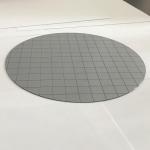
2inch 3inch 4inch 5inch 6inch 8inch 12inch FZ CZ N-type polished silicon wafer DSP SiO2 wafers Silicon oxide wafer 1inch 2inch 10x10mm Scanning ...
2025-05-06 20:44:47
|
|
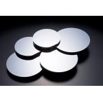
6inch 8inch 2inch 1inch FZ CZ N-type polished silicon wafer DSP SiO2 wafers Silicon oxide wafer Polished Silicon Wafer High-purity (11N) 1-12 inch ...
2025-05-06 20:44:51
|
|
... substrate sapphire window sapphire wafer Applications of AlN template Silicon-based semiconductor technology has reached its limits and could not ...
2025-05-06 20:44:39
|
|
...Substrate 111 P Type N Type for Micro-electromechanical systems (MEMS) Or Power semiconductor devices Or Optical components and sensors Product ...
2025-05-06 20:45:50
|
|
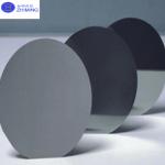
... Silicon Wafer Silicon wafers are the backbone of the semiconductor industry, serving as the fundamental substrate for integrated circuits, ...
2025-05-06 20:45:52
|
|
... Silicon on Insulator (SOI) is an advanced semiconductor technology where a thin insulating layer, typically silicon dioxide (SiO₂), is inserted ...
2025-05-06 20:45:55
|