
111 - 120 of 166
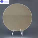
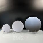
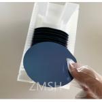
40x3mmt silicon carbon wafers
Selling leads
|
...Wafer 6inch 150mm SiC type 4H-N Si type N or P N-type SiC on Si Compound Wafer abstract N-type silicon carbide (SiC) on silicon (Si) compound ...
2025-05-06 20:45:18
|
|
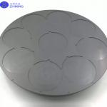
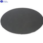
silicon carbide ceramic tray Used to support materials semiconductor wafers Excellent corrosion resistance. silicon carbide ceramic tray‘s short brief ...
2025-05-06 20:47:46
|
|
...wafer P Type N Type 6 inch 8 inch 12 inch Surface polish SSP/DSP Abstract of SOI wafer Silicon on Insulator (SOI) is an advanced semiconductor ...
2025-05-06 20:45:55
|
|
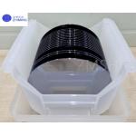
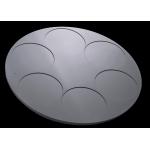
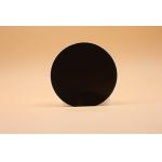
...Silicon Carbide SiC Coated Graphite Tray High Temperature Resistance Graphite Plates Silicon carbide coated epitaxial sheet tray used in epitaxial ...
2025-05-06 20:47:41
|
|
Silicon wafer Conductivity Solar Cells Solar Cells Power Semiconductor Devices High Purity Product Description: Attributes Details Substrate Material ...
2025-05-06 20:45:09
|
|
...Wafer with (111) Crystal Orientation – Introduction The 8-inch silicon wafer with (111) crystal orientation is a vital component in the semiconduct...
2025-05-06 20:45:52
|
|
AlN on Diamond template wafers AlN epitaxial films on Diamond substrate AlN on Sapphire /AlN-on-SiC/ AlN-ON Silicon Welcome to Know AlN Template on ...
2025-05-06 20:44:22
|
|
...wafers for Thermal management area According to statistics, the temperature of the working junction will drop Low 10 ° C can double the device life...
2025-05-06 20:44:23
|
|
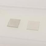
SiO2 wafer Thermal Oxide Laver Thickness 20um+5% MEMS Optical Communication System Product Description: The SIO2 silicon dioxide wafer serves as a ...
2025-05-06 20:45:05
|
|
...Wafer (Lithium Niobate on Insulator)2/3/4/6/8 Inch Si/LN Substrate Introduction of LNOI Wafer LNOI (Lithium Niobate on Insulator) wafers are a ...
2025-06-30 20:10:46
|