
71 - 80 of 166
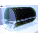
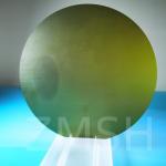
40x3mmt silicon carbon wafers
Selling leads
|
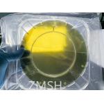
... a cutting-edge material widely used in power electronics and advanced semiconductor applications. Silicon carbide, particularly the 4H polytype, ...
2025-05-06 20:41:52
|
|
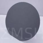
2inch 4inch 6inch 8inch 3C-N SiC Wafer Silicon Carbide Optoelectronic High-Power RF LEDS Description of 3C-N SiC Wafer: Compared to 4H-Sic, although ...
2025-05-06 20:41:48
|
|
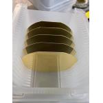
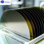
... Polished Silicon Wafer High-purity (11N) 1-12 inch single- and double-polished Czochralski wafers Sizes 1" 2" 3" 4" 5" 6" 8" 12" and special size ...
2025-05-06 20:44:51
|
|
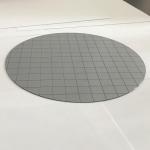
...silicon wafer DSP SiO2 wafers Silicon oxide wafer 1inch 2inch 10x10mm Scanning electron microscope silicon wafer small square piece SEM Polished ...
2025-05-06 20:44:47
|
|
... Wafer thickness 500±25um n doped dummy prime research grade 8inch 12inch 4H-N type SiC Wafer's abstract This study presents the characterization ...
2025-05-06 20:41:22
|
|
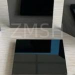
... substrates that play a crucial role in various semiconductor applications. Commonly used in compact electronic devices where space is limited. ...
2025-05-06 20:41:38
|
|
..., is a critical material in the semiconductor industry due to its exceptional thermal conductivity, high breakdown voltage, and superior mechanical ...
2025-05-06 20:41:55
|
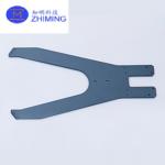
SiC Wafer Hand for Wafer Handling, Cleanroom Compatible, Corrosion Resistant, Customizable Interface
|
Product Introduction of Wafer Hand The SiC wafer hand is an end-effector designed for handling wafers with high hardness and thermal stability. ...
2025-05-29 00:09:29
|
|
4H SiC Seed Wafer Thickness 600±50μm Customization Silicon carbide growth Description of SiC Seed Wafer: SiC seed crystal is actually a small crystal ...
2025-05-06 20:41:47
|

|
6H-N Semi-insulating SiC substarte/wafer for MOSFETs,JFETs BJTs,high resistivity wide bandgap Semi-insulating SiC substarte/wafer's abstract Semi...
2025-05-06 20:41:20
|