
231 - 240 of 329
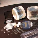
piezoelectric sensors lgs wafer
Selling leads
|
... recording, and frequency conversion because of its electro-optic,acousto-optic,piezoelectric,thermal-optic and photorefractive effects. With the ...
2025-07-30 00:13:57
|
|
4 Inch Lithium Niobate Wafer Polished 128Y 36Y For SAW Applications Lithium Niobate is a ferroelectric material suitable for a variety of applications...
2025-07-30 00:13:57
|
|
Fe doped Lithium Niobate Wafer Optical Grade and SAW Grade Lithium Niobate (LiNbO3) is a useful optoelectronic material. The material not only has ...
2025-07-30 00:13:57
|
|
Ultra-Thin LiTaO3 Wafer Z-Cut For Pyroelectric Infrared Detector Lithium tantalite (LiTaO3) presents unique electrooptical, acoustic, piezoelectric, ...
2024-12-09 20:56:33
|
|
... Wafer used in Visible, Near-Infrared and Mid-Infrared Regions Lithium niobate is transparent between 0.25 and 5.3 μm. It can be used in visible, ...
2025-07-30 00:13:57
|
|
...-cut, CT-cut, DT-cut, X-cut and Y-cut. They are used for production of quartz crystal units, quartz crystal filters, piezoelectric transducers and ...
2025-07-30 00:13:57
|
|
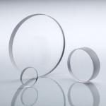
2 Inch Sapphire Crystal C Plane Polished Sapphire Wafers Sapphire Substrates Specification: Single crystal Al2O3 99.999% Orientation: R-axis 0.5° ...
2024-12-09 21:21:54
|
|
High Resistance Sapphire Polished Wafer 3 Inch C-Plane Optical Crystal Sapphire is a single crystal of alumina and is the second-hardest material in ...
2024-12-09 21:35:54
|
|
2 Inch 4 Inch 6 Inch Sapphire Single Crystal Wafer With Various Orientations Sizes: 2 ", 4 ", 6 "and cut small pieces; C direction, M direction, R ...
2024-12-09 21:37:23
|
|
10mm Square SrTiO3 Crystal Wafer For Semiconductor SrTiO3 single crystal has the good lattice structure of perovskite structure materials. For the ...
2024-12-09 21:42:24
|