
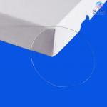
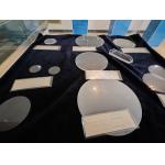
2 Inch C Plane Polished Sapphire Wafers Crystal Substrates
|
|
2 Inch Sapphire Crystal C Plane Polished Sapphire Wafers Sapphire Substrates
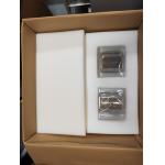
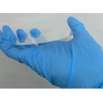
Specification: Diameter:50.8±0.1mm Thickness :430±15um or 330±15um Primary flat:16±1mm OF Orientation flat: Off R to C axis 45°±0.1° C-plane(0001) Frontside Surface Roughness:Ra<0.2nm Backside Surface Roughness: 0.8~1.2um ( Or double side polished, both side Ra<0.2nm) TTV:<10um BOW:-10~0um WARP:<10um Laser Mark Series No. by needs Package:Vacuum-sealed containers with nitrogen backfill in a class 100 environment Cleanliness :Free visible contamination
1. Sapphire has a high optical transmittance, so it is widely used as microelectronic tube dielectric material, ultrasonic conduction element, waveguide laser cavity, and other optical elements, as window materials for infrared military devices, space vehicles, high-intensity lasers and optical communications. 2. Sapphire has high rigidity, high strength, high working temperature, abrasion resistance, corrosion resistance characteristics, so sapphire substrate is often used in harsh environments, such as boiler water gauge (high-temperature resistance), commodity bar code scanner, bearing, and other precision manufacturing (wear resistance), coal, gas, well detection sensors and detector windows (anti-corrosion). 3. Sapphire has the characteristics of electrical insulation, transparency, good thermal conductivity, and high rigidity, so it can be used as the substrate material of integrated circuits, such as LED and microelectronic circuits, ultra-high-speed integrated circuit.
Acceptance Check |
||||||||||||||||||||||||||||||||||||||||||
| Product Tags: Polished Sapphire Crystal Wafer C Plane Polished Sapphire Wafers 2 Inch Sapphire Substrates Wafers | ||||||||||||||||||||||||||||||||||||||||||
|
Stoichiometric LiTaO3 Wafers Ideal Material for Optical Modulators and Frequency Converters |
|
3" 4" 6" Single Crystal Quartz With Customized Wafers And Their Outstanding Material Properties |
|
3" 4" 6"Single Crystal Quartz Wafers For High Temperature Applications Customized Orientation Options With 3 Inch And 4 Inch Sizes |
|
3 Inch And 4 InchCustomized Orientation Options For Single Crystal Quartz Wafer High Temperature |
|
Stoichiometric LiTaO3 Wafers The Ultimate Choice for High-Frequency Electronics |
|
2" 3" 4" 6" Lithium Tantalate Wafers Ultimate Solution For Piezoelectric Applications |