
101 - 110 of 243
photonic applications mgo wafers
Selling leads
|
... and the reverse effect can also happen. Piezoelectric materials have non-conductive nature and they can be classified as ceramics and crystals. ...
2024-12-09 20:34:25
|
|
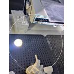
...Wafer SAW Application IDT use Ra Roughness 1nm The reduction technology is used to produce Black Lithium Niobate (LiNbO3) which has high ability to ...
2024-12-09 20:34:25
|
|
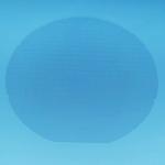
...Wafer For Electronics, Optics, And Semiconductors Borofloat 33 Glass Wafer Description Borofloat 33 is a type of borosilicate glass that is widely ...
2024-12-09 22:13:23
|
|
... coefficient of thermal expansion. It has a wide range of uses including optical components, semiconductor wafers and microelectronic components. ...
2024-12-09 22:58:07
|
|
...Applications: LiTaO3 in Biomedical Sensing In the realm of biomedical sensing, LiTaO3 emerges as a game-changer, driven by its pyroelectric effect ...
2024-12-09 22:59:53
|
|
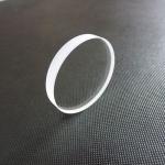
.... It has an orientation of ±0.5°, a wafer shape, a clear aperture of greater than 90%, and TTV of ≤3μm. It is also customizable in size to meet the ...
2024-12-09 23:10:26
|
|
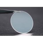
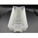
...Wafer with BOW 10um Product Description: Sapphire Wafer is a kind of sapphire slice that has been precision cut from a sapphire boule to the ...
2024-12-09 23:10:26
|
|
...Wafer ≤3 Arc Min Perpendicularity Parallelism ≤3 Arc Sec Product Description: Sapphire Wafer is an ideal choice for high-end applications due to ...
2024-12-09 23:10:26
|
|
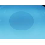
... 33 Glass Wafer for Optimal Performance in Electronics Borofloat 33 Glass Wafer Description Borofloat 33 - the ultimate choice for precision optics ...
2024-12-09 23:27:58
|
|
... Silica Wafer 3'' 4'' 6'' JGS1 JGS2 JGS3 for Glass and Quartz Materials The Epitome of Optical Clarity and Precision Elevate your optical ...
2025-07-17 00:19:03
|