
61 - 70 of 243
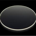
photonic applications mgo wafers
Selling leads
|
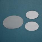
... with surface quality of single side polished, total thickness variation of less than 3μm, wafer shape, and clear aperture of more than 90%. The ...
2024-12-09 23:10:26
|
|
...Wafer is a type of semiconductor material made of sapphire, which has excellent optical, mechanical, and chemical properties. It is commonly used ...
2024-12-09 23:27:58
|
|
...Wafer Sapphire Wafer 330um 430um Thick Our sapphire wafers are the epitome of precision and quality, crafted from the purest sapphire crystal. ...
2024-12-09 20:34:25
|
|
... applications. Crafted from the purest fused silica, our wafers offer unparalleled optical clarity, thermal stability, and chemical resistance. ...
2024-12-10 00:15:50
|
|
... wafers this is the Kyropoulos method (abbreviated to Ky or Kr). The Kyropoulos method is a continuation of the Czochralski method (CZ) which is ...
2024-12-09 20:34:25
|
|
...Wafer for Semiconductor and MEMS Applications The piezoelectric effect in a crystal is explained as that there will be the development of electric ...
2025-07-16 00:18:07
|
|
..., filters, transducers, high-frequency surface acoustic wave devices, as well as bulk acoustic devices. Material Characteristics Material 3" 4" 6" ...
2025-07-16 00:18:07
|
|
... in various electronic and optical applications. These synthetic quartz exhibits exceptional properties such as high purity, excellent electrical ...
2025-07-16 00:18:07
|
|
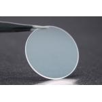
...Wafer - Perfect for demanding applications Product Description: Sapphire Wafer is a kind of sapphire plate made from high quality sapphire ...
2024-12-09 23:10:26
|

|
...Wafers The Ultimate Material for Your Most Demanding Applications the power of innovation with our premium Quartz Wafers, the cornerstone of ...
2025-07-16 00:18:07
|