
161 - 170 of 311
lithography etching piezoelectric wafers
Selling leads
|
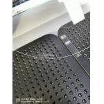
3" 4" 6" 8" Lithium Niobate Wafer Excellent Electro-Optic and Piezoelectric Properties The Ultimate Material for Advanced Applications Unlock the ...
2024-12-09 23:27:58
|
|
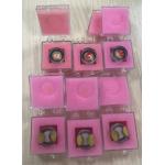
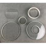
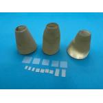
Precision-Engineered for Your Instrumentation System Our Piezoelectric Quartz End Cap Revolutionary Quartz End Caps: Elevating Your Device Performance...
2024-12-10 00:15:50
|
|
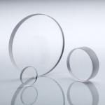
2 Inch Sapphire Crystal C Plane Polished Sapphire Wafers Sapphire Substrates Specification: Single crystal Al2O3 99.999% Orientation: R-axis 0.5° ...
2024-12-09 21:21:54
|
|
High Resistance Sapphire Polished Wafer 3 Inch C-Plane Optical Crystal Sapphire is a single crystal of alumina and is the second-hardest material in ...
2024-12-09 21:35:54
|
|
High Durability High Resistance Sapphire Substrate Round Wafer Sapphire is used for its durability and erosion/corrosion resistance, often in ...
2024-12-09 21:35:54
|
|
2 Inch 4 Inch 6 Inch Sapphire Single Crystal Wafer With Various Orientations Sizes: 2 ", 4 ", 6 "and cut small pieces; C direction, M direction, R ...
2024-12-09 21:37:23
|
|
10mm Square SrTiO3 Crystal Wafer For Semiconductor SrTiO3 single crystal has the good lattice structure of perovskite structure materials. For the ...
2024-12-09 21:42:24
|
|
10mm Square Fe Doped SrTiO3 Crystal Wafer For Semiconductor Fe-doped strontium titanate (SrTiO3) and strontium titanate single crystal have similar ...
2024-12-09 21:42:24
|
|
10mm Square Fe Doped SrTiO3 Crystal Wafer Used As Optical Windows Nb doped strontium titanate (Nb:SrTiO3) has similar structure to strontium titanate ...
2024-12-09 21:42:24
|
|
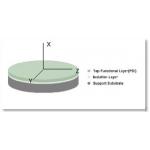
Achieving Compact Photonic Integration With 4-Inch LNOI Wafers LNOI stands for Lithium Niobate on Insulator, which is a specialized substrate ...
2025-07-15 00:17:51
|