
121 - 130 of 288
high performance mgo wafers
Selling leads
|
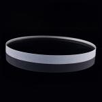
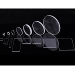
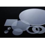
... in the VIS and UV is approx. The transmission range of significantly cheaper JGS2 wafers is shifted towards longer wavelengths when compared with ...
2024-12-09 20:34:25
|
|
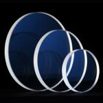
..., the melting method Synthetic CVD. Fused silica is highly heat resist and has a broad transmission range (>85% @185nm, >90% from 200nmto 2000nm). ...
2024-12-09 20:34:25
|
|
... even if the electric potential occurs instantaneously. The pyroelectric effect of LN wafer is almost eliminated and the transmittance is ...
2025-07-22 00:23:46
|
|
... applications. Our standard wafer diameters range from 25.4 mm (1 inch) to 150 mm (6 inches) in size. Lithium Tantalate (LiTaO3), also known as LN ...
2025-07-22 00:23:46
|
|
... are made from high-purity lithium niobate crystals and offer several advantages due to their larger size. Here is a description of 8-inch LiNbO3 ...
2024-12-09 22:36:19
|
|
.... Fused Silica Wafer has very low thermal expansion coefficient, excellent electrical insulation properties, and superior thermal shock resistance. ...
2024-12-09 22:58:07
|
|
...TTV of ≤3μm, thickness of 0.5mm-3mm and roundness of edge grinding. With its high-end material and strict quality control, Sapphire Wafer provides ...
2024-12-09 23:10:26
|
|
...Wafer for Miniature Electronic Devices the Sapphire Crystal Wafer - a cutting-edge material that revolutionizes optical, electronic, and semiconduc...
2024-12-09 23:27:58
|
|
...Wafer for High Frequency Broadband Filter and Piezoelectric Transducer The electromechanical coupling coefficient of LiTaO3 crystals is large, and ...
2024-12-09 21:17:37
|
|
... transmittance, high strength, collision resistance, wear resistance, corrosion resistance and high temperature and high pressure resistance, ...
2024-12-09 21:35:54
|