
161 - 170 of 345
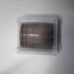
high frequency electronics wafers
Selling leads

|
... materials, engineered to deliver superior stability and efficiency for cutting-edge applications. By incorporating 5mol% magnesium oxide (MgO) ...
2026-03-27 20:05:03
|

|
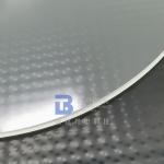
... (SiO₂) to deliver exceptional optical clarity, thermal stability, and chemical resistance. Ideal for laser systems, photomasks, semiconductor ...
2026-03-27 20:05:03
|
|
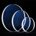
...Wafers Used In Semiconductor, Optical, Medical, Military, Photonic Industry BonTek can make transparent glass wafers from any available glass brand...
2026-04-20 00:26:01
|
|
... in the VIS and UV is approx. The transmission range of significantly cheaper JGS2 wafers is shifted towards longer wavelengths when compared with ...
2026-03-27 20:05:03
|
|
..., the melting method Synthetic CVD. Fused silica is highly heat resist and has a broad transmission range (>85% @185nm, >90% from 200nmto 2000nm). ...
2026-03-27 20:05:03
|

|
...Wafer for Superior SAW Device Performance Lithium niobate wafers are revolutionizing the optical technology industry with their unique combination ...
2026-03-27 20:05:03
|
|
... even if the electric potential occurs instantaneously. The pyroelectric effect of LN wafer is almost eliminated and the transmittance is ...
2026-04-20 00:26:01
|
|
... applications. Our standard wafer diameters range from 25.4 mm (1 inch) to 150 mm (6 inches) in size. Lithium Tantalate (LiTaO3), also known as LN ...
2026-04-20 00:26:01
|
|
.... Fused Silica Wafer has very low thermal expansion coefficient, excellent electrical insulation properties, and superior thermal shock resistance. ...
2026-03-27 20:05:03
|
|
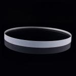
...TTV of ≤3μm, thickness of 0.5mm-3mm and roundness of edge grinding. With its high-end material and strict quality control, Sapphire Wafer provides ...
2026-03-27 20:05:03
|