
141 - 150 of 345
high frequency electronics wafers
Selling leads
|
.... Stoichiometric LiTaO3, renowned for its exceptional ferroelectric, piezoelectric, and electro-optic properties, is the go-to material for cutting...
2026-03-27 20:05:03
|
|
...Wafer The Optimal Solution for High-Temperature Superconducting YBCO Research and Production Experience the unparalleled advantages of our LaSrAlO4 ...
2026-03-27 20:05:03
|
|
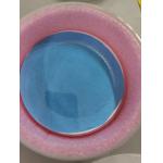
... Quartz Wafers for High Temperature Applications Customized Orientation Options with 3 Inch and 4 Inch Sizes our Single Crystal Quartz Wafers, the ...
2026-04-20 00:26:01
|
|
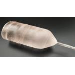
.... Renowned for their outstanding properties, they are the go-to choice for a multitude of industries. Our sapphire wafers are engineered to ...
2026-03-27 20:05:03
|
|
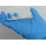
...Wafer for High-Performance Semiconductor Device Production In the realm of advanced materials, our fused silica wafers shine as a cornerstone for ...
2026-03-27 20:05:03
|
|
... component must meet the strictest standards. That's where our Fused Silica Wafers shine, offering a level of quality and performance that sets ...
2026-03-27 20:05:03
|
|
... applications? Look no further than our LaSrAlO₄ crystal wafers. These wafers are crafted with utmost precision, ensuring exceptional crystal ...
2026-03-27 20:05:03
|
|
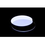
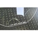
...Glass Wafers The Innovative and High-Performance Choice for Your Applications Available in Multiple Sizes Are you in pursuit of the ideal substrate ...
2026-03-27 20:05:03
|
|
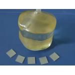
High-Sensitivity Signal Processing with Our Precision Stoichiometric LiNbO3 Piezoelectric Wafer for Optoelectronic Applications Elevate your research ...
2026-03-27 20:05:03
|

|
...Wafers Engineered for Peak Thermal Stability, Exceptional Chemical Resistance, and Ultra-High Optical Clarity For industries requiring high...
2026-03-27 20:05:03
|