
111 - 120 of 345
high frequency electronics wafers
Selling leads
|
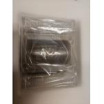
...Wafer As Carrier Wafers Due to their low thickness, thin wafers are vulnerable to stress and breakage. Warping of the wafers during handling and ...
2026-04-20 00:26:01
|
|
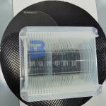
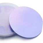
...Wafer 36Y 42Y For SAW and BAW Applications Lithium Tantalate (LiTaO3) is an ideal material for both SAW and optical use. It has relatively large ...
2026-03-27 20:05:03
|
|
LiNbO3 LiTaO3 Quartz Piezoelectric Wafer for Higher Frequency SAW Devices Piezoelectric Wafer Description The basic principle of SAW devices is the ...
2026-03-27 20:05:03
|
|
... applications. Crafted from the purest fused silica, our wafers offer unparalleled optical clarity, thermal stability, and chemical resistance. ...
2026-03-27 20:05:03
|
|
...our premium LiNbO3 Wafers, the cornerstone for cutting-edge photonic and electro-optic applications. As a leading supplier, we offer LiNbO3 Wafers ...
2026-03-27 20:05:03
|
|
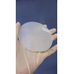
...high quality sapphire single crystal. It has the characteristics of bow and warp ≤ 20μm, TTV ≤ 3μm, clear aperture > 90%, diameter range from 2inch ...
2026-03-27 20:05:03
|
|
... applications requiring unmatched optical clarity and thermal stability. Crafted from high-purity silica glass through a meticulous fusion process, ...
2026-03-27 20:05:03
|
|
High Chemical Resistance Borosilicate Glass Wafer 4'' 6'' 8'' for MEMS Devices Glass wafers made of borosilicate glass are often used in Semiconductor ...
2026-03-27 20:05:03
|
|
... ingots to wafer processing. We have established the supply system mainly for the mass-produced wafers for bipolar integrated circuits, discrete ...
2026-03-27 20:05:03
|
|
...Silicon Wafer With High Resistivity For Semiconductor Silicon wafers are thin slices of pure crystalized silicon. These pure forms of wafers are ...
2026-03-27 20:05:03
|