
191 - 200 of 459
customized wafers quartz wafer
Selling leads
|
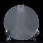
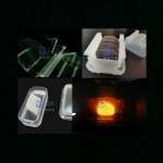
...anti-abrasion, good thermal conductivity, and good electrical isolation. Due to its excellent mechanical and chemical characteristics, the sapphire ...
2026-03-27 20:05:03
|
|
...Wafer for Higher Frequency SAW devices Free-pyro black LiNbO3 and LiTaO3 wafers were prepared successfully by chemical reduction under a mixed ...
2026-03-27 20:05:03
|
|
...Wafer Free-pyro for Higher Frequency SAW devices The pyroelectric effect for the black LiNbO3 and LiTaO3 wafers was almost eliminated and the ...
2026-03-27 20:05:03
|

|
...Wafer for Superior SAW Device Performance Lithium niobate wafers are revolutionizing the optical technology industry with their unique combination ...
2026-03-27 20:05:03
|
|
...Wafer for Surface Acoustic Wave IDT Applications Free-pyro black LiNbO3 and LiTaO3 wafers were prepared successfully by chemical reduction under a ...
2026-03-27 20:05:03
|
|
... even if the electric potential occurs instantaneously. The pyroelectric effect of LN wafer is almost eliminated and the transmittance is ...
2026-04-19 00:24:26
|
|
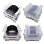
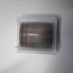
12 inch Silicon Wafer Prime Test Dummy Wafers Silicon wafer is a material used for producing semiconductors, which can be found in all types of ...
2026-03-27 20:05:03
|
|
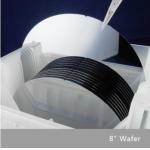
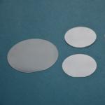
... applications. Our standard wafer diameters range from 25.4 mm (1 inch) to 150 mm (6 inches) in size. Lithium Tantalate (LiTaO3), also known as LN ...
2026-04-19 00:24:26
|
|
... with surface quality of single side polished, total thickness variation of less than 3μm, wafer shape, and clear aperture of more than 90%. The ...
2026-03-27 20:05:03
|
|
...TTV of ≤3μm, thickness of 0.5mm-3mm and roundness of edge grinding. With its high-end material and strict quality control, Sapphire Wafer provides ...
2026-03-27 20:05:03
|