
221 - 230 of 459
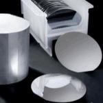
customized wafers quartz wafer
Selling leads

|
..., our 5mol% MgO-Doped Lithium Niobate (LiNbO₃) Wafers are engineered to deliver superior electro-optic, acoustic, and nonlinear optical properties. ...
2026-03-27 20:05:03
|
|
...Wafer SAW Application IDT use Ra Roughness 1nm The reduction technology is used to produce Black Lithium Niobate (LiNbO3) which has high ability to ...
2026-03-27 20:05:03
|
|
...Wafer Nonlinear Optical Crystals For E-O Devices LiTaO3 is an E-O crystal widely used for E-O devices, due to its good optical NLO and E-O ...
2026-03-27 20:05:03
|
|
...Wafer 36°, 39°, 42 °, 46°, 48°, X-CUT used for Surface Acoustic Wave Devices Lithium tantalate (LiTaO3), has properties which make it useful for ...
2026-03-27 20:05:03
|
|
... Fused Silica Wafer 4'' 6'' 500um SiO2 HPFS with Excellent Chemical Resistance Fused Silica (SiO2) wafers are made from high purity fused silica, ...
2026-03-27 20:05:03
|
|
... range (>85% @185nm, >90% from 200nmto 2000nm). The most seen brand/grade is JGS1, Corning 7980 and SK1300. BonTek supply these wafers with ...
2026-04-19 00:24:26
|
|
...Wafer JGS3 C7979 and SK1310 with Very Low OH content There are also IR grade Fused Silica wafers with transmission from 185nm to 350nm. The IR ...
2026-03-27 20:05:03
|
|
...an ideal material for Anodic bonding. BonTek provides borosilicate wafers from 2 to 14 inches diameter, the thickness is 100um up with low ...
2026-03-27 20:05:03
|
|
...Wafer with A-plane 11-20 Primary Flat Our sapphire wafers are precision-crafted using the finest materials and cutting-edge technology. Sapphire, a ...
2026-03-27 20:05:03
|
|
...r specific requirements are met by choosing prime grade and defecting free silicon wafer as a substrate so that a high uniform layer of thermal ...
2026-04-19 00:24:26
|