
161 - 170 of 459
customized wafers quartz wafer
Selling leads
|
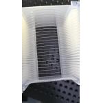
Customized 6 Inch 8 Inch Piezoelectric Wafer for POI Applications and MEMS Piezoelectric effect is defined as the change in electric polarization of ...
2026-03-27 20:05:03
|
|
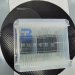
Customized doping percent LiNbO3 Wafer MgO Er Fe doped Optical grade or SAW grade Lithium Niobate (LiNbO3) is a useful optoelectronic material. The ...
2026-03-27 20:05:03
|

|
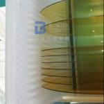
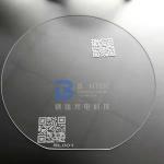
4 Inch Lithium Niobate Wafer with Customized Orientation Cut for Various Designs The Premier Material for Precision Instrumentation LiNbO3, a leading ...
2026-04-19 00:24:26
|
|
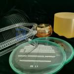
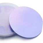
...Wafer Sapphire Wafer 330um 430um Thick Our sapphire wafers are the epitome of precision and quality, crafted from the purest sapphire crystal. ...
2026-03-27 20:05:03
|
|
...piezoelectric materials. Developed by our team of experts, these wafers are made from Langasite Crystal and have superior performance compared to ...
2026-03-27 20:05:03
|
|
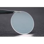
... applications. Crafted from the purest fused silica, our wafers offer unparalleled optical clarity, thermal stability, and chemical resistance. ...
2026-03-27 20:05:03
|
|
...Wafer 4'' 6'' 8'' for MEMS Devices Glass wafers made of borosilicate glass are often used in Semiconductor and MEMS industry in a wide variety of ...
2026-03-27 20:05:03
|
|
...Wafers Thickness 0.35±0.025mm in Fused Silica Borosilicate BonTek is a recognized participant in the manufacture of transparent Glass wafers. Many ...
2026-03-27 20:05:03
|
|
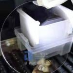
... ingots to wafer processing. We have established the supply system mainly for the mass-produced wafers for bipolar integrated circuits, discrete ...
2026-03-27 20:05:03
|
|
...Silicon Wafer With High Resistivity For Semiconductor Silicon wafers are thin slices of pure crystalized silicon. These pure forms of wafers are ...
2026-03-27 20:05:03
|