
101 - 110 of 116
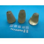
al2o3 substrate sapphire wafer
Selling leads
|
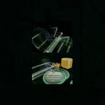
X-cut and Z-cut LiNbO3 wafer 8 inch Large Size For Optical Use Lithium niobate is transparent between 0.25 and 5.3 μm. It can be used in visible, near ...
2025-07-31 00:19:35
|
|
...Wafer Z-Cut For Pyroelectric Infrared Detector Lithium tantalite (LiTaO3) presents unique electrooptical, acoustic, piezoelectric, pyroelectric and ...
2024-12-09 20:56:33
|
|
... SrTiO3 Crystal Wafer For Semiconductor SrTiO3 single crystal has the good lattice structure of perovskite structure materials. For the epitaxial ...
2024-12-09 21:42:24
|
|
...Wafer For Semiconductor Fe-doped strontium titanate (SrTiO3) and strontium titanate single crystal have similar structure. Strontium titanate ...
2024-12-09 21:42:24
|
|
...Wafer Used As Optical Windows Nb doped strontium titanate (Nb:SrTiO3) has similar structure to strontium titanate single crystal, but Nb:SrTiO3 has ...
2024-12-09 21:42:24
|
|
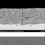
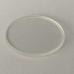
Product Description: Fused Silica Wafer is a kind of Calcium Silicate Board, also known as Glass Wafer. It is a precision engineered and manufactured ...
2024-12-09 22:58:07
|
|
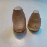
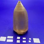
Enhance Your Applications with the Exceptional Electrical Optical and Mechanical Properties of MgO Single Crystal Substrate Elevate your research and ...
2025-07-26 00:13:26
|
|
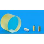
Enabling High-Speed Modulation And Wide Bandwidth With LNOI POI Piezo on Insulation (POI) refers to a technology where piezoelectric materials are ...
2025-07-31 00:19:35
|
|
6 inch 0.5mm Borofloat 33 Glass Substrate for Semiconductor Industry and MEMS With its unique physical and chemical properties, BOROFLOAT33 has become ...
2024-12-09 20:34:25
|
|
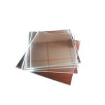
Customized Square Shape Borofloat 33 Glass Substrate with a wide range of uses BOROFLOAT33 is a high quality borofloat glass with excellent properties ...
2024-12-09 20:34:25
|