
High Speed Modulation And Wide Bandwidth Piezoelectric Wafer With LNOI POI
|
|
Enabling High-Speed Modulation And Wide Bandwidth With LNOI POI
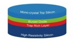
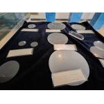
Piezo on Insulation (POI) refers to a technology where piezoelectric materials are integrated onto an insulating substrate. This allows for the utilization of the piezoelectric effect while providing electrical isolation. The POI technology enables the development of various devices and systems that harness the unique properties of piezoelectric materials for sensing, actuation, and energy harvesting applications.
POI (Piezo on Insulation) technology finds various applications in different fields due to its ability to combine the advantages of piezoelectric materials with electrical isolation. Such as sensors, Microelectromechanical Systems and Energy Storage and Generation.
The versatility of integrating piezoelectric materials onto an insulating substrate opens up possibilities for innovative solutions in diverse fields, including electronics, energy, healthcare, and more.
|
||||||||||||||||||||||||||||||||||||||||||||||||||||||||||||||||||||||||||||
| Product Tags: High Speed Modulation Piezoelectric Wafer Wide Bandwidth Piezoelectric Wafer LNOI POI Piezoelectric Wafer | ||||||||||||||||||||||||||||||||||||||||||||||||||||||||||||||||||||||||||||
|
Stoichiometric LiTaO3 Wafers Ideal Material for Optical Modulators and Frequency Converters |
|
3" 4" 6" Single Crystal Quartz With Customized Wafers And Their Outstanding Material Properties |
|
3" 4" 6"Single Crystal Quartz Wafers For High Temperature Applications Customized Orientation Options With 3 Inch And 4 Inch Sizes |
|
3 Inch And 4 InchCustomized Orientation Options For Single Crystal Quartz Wafer High Temperature |
|
Stoichiometric LiTaO3 Wafers The Ultimate Choice for High-Frequency Electronics |
|
2" 3" 4" 6" Lithium Tantalate Wafers Ultimate Solution For Piezoelectric Applications |