
61 - 70 of 115
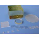
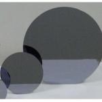
al2o3 substrate sapphire wafer
Selling leads
|
..., a premium material known for its exceptional electrical, optical, and mechanical properties. Ideal for a wide range of applications, MgO Single ...
2025-03-06 16:31:06
|
|
... applications demanding unmatched optical transparency, excellent electrical insulation, and superior mechanical strength. These wafers are ...
2025-03-06 16:31:03
|
|
...Crystal Substrate Tight Dimensional Tolerance and Ultra-Smooth Surfaces for Optimal Performance our ZnO (Zinc Oxide) Wafers, the pinnacle of ...
2025-03-06 16:31:03
|
|
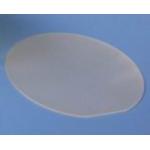
... or wafer made from a thin layer of LiNbO3 material. Size: The thin film has a diameter of 3 inches, which is equivalent to approximately 76 ...
2024-12-09 22:36:19
|
|
... or wafer made from a thin layer of LiTaO3 material. Size: The thin film has a diameter of 3 inches, which is equivalent to approximately 76 ...
2025-07-24 00:21:42
|
|
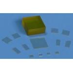
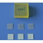
...Wafer 4'' 6'' 8'' for MEMS Devices Glass wafers made of borosilicate glass are often used in Semiconductor and MEMS industry in a wide variety of ...
2024-12-09 20:34:25
|
|
...Wafers Corning 7980 in stock for Immediate Shipment High quality 4 inch SiO2 Fused Silica wafers are in stock for immediate shipment. Order 100mm ...
2024-12-09 20:34:25
|
|
.... Such wafers are most commonly specified as 3" diameter with a reference flat. Wafer orientation is customer specified based on desired component ...
2025-07-24 00:21:42
|
|
... electronics. BonTek offers Prime, Test, Monitor, SEMI standard, and customized silicon wafers in all diameters from 2″ to 300mm. Our silicon ...
2024-12-09 20:34:25
|
|
ZnO crystal substrate is used in GaN(blue LED) epitaxial substrate wide band connection devices and other fields Zinc oxide (ZnO) crystal substrate is ...
2024-12-10 00:32:09
|