1 - 10 of 136
12 inch semiconductor wafer
Selling leads|
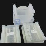
12 inch Silicon Wafer Prime Test Dummy Wafers Silicon wafer is a material used for producing semiconductors, which can be found in all types of ...
2024-12-09 21:18:07
|
|
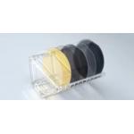
Product Description: Fused Silica Wafer is an optical-grade monocrystalline wafer made of quartz material, also known as fused quartz or fused silica. ...
2024-12-09 22:58:07
|
|
... of people. Silicon comes second as the most common element in the universe; it is mostly used as a semiconductor in the technology and electronic ...
2024-12-09 21:18:07
|
|
... properties and thermal stability. It is widely used in various industries, including optics, lasers, semiconductors, and scientific research. JGS1 ...
2025-07-24 00:21:42
|
|
Customized 6 Inch 8 Inch Piezoelectric Wafer for Semiconductor POI and MEMS Positive piezoelectric effect (direct piezoelectric effect) : The ...
2024-12-09 20:34:25
|
|
...an ideal material for Anodic bonding. BonTek provides borosilicate wafers from 2 to 14 inches diameter, the thickness is 100um up with low ...
2024-12-09 20:34:25
|
|
...Inch 6-Inch LNOI Wafers The Perfect Choice for Compact and High-Performance Optical Communication Revolutionize Photonics with Ultra-Low-Loss LNOI ...
2025-05-29 14:33:33
|
|
...Inch LiNbO3 Wafer Polished 0.25mol% Er Dope Or 5mol% MgO Dope For Optical Applications Doped LN Wafers: Er:LN, MgO:LN, and Fe:LN Doping lithium ...
2025-07-24 00:21:42
|
|
Compound Semiconductors Lithium Tantalate Wafer used for Optical Devices, SAW Devices Compound semiconductors are the semiconductors composed of more ...
2025-07-24 00:21:42
|
|
.... If the charge distribution is not symmetrical, the net polarization will appear, and an electric field will be generated, which is the piezoelect...
2024-12-09 20:34:25
|


