
11 - 20 of 136
12 inch semiconductor wafer
Selling leads
|
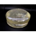
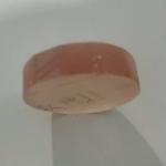
...Inch LiNbO3 Wafer Polished 5mol% MgO Dope For Magnetic and Optical Applications Elevating Performance in Optical & Electronic Applications ...
2025-07-30 00:13:57
|
|
Customized 6 Inch 8 Inch Piezoelectric Wafer for POI Applications and MEMS Piezoelectric effect is defined as the change in electric polarization of ...
2024-12-09 20:34:25
|
|
3 inch to 8 inch Piezoelectric Wafer with Laser Marking for Surface Acoustic Wave Use The piezoelectric effect, discovered in 1880 by Pierre and ...
2025-06-21 11:31:50
|

|
Large Diameter 8 inch LiNbO3 wafers 128°Y-cut and Z-cut For Surface Acoustic Wave Devices Lithium Niobate (LiNbO3) is colorless or slightly yellowish ...
2025-07-30 00:13:57
|
|
Achieving Compact Photonic Integration With 4-Inch LNOI Wafers LNOI stands for Lithium Niobate on Insulator, which is a specialized substrate ...
2025-07-30 00:13:57
|
|
4 Inch LiTaO3 Wafer with High Refractive Index for SAW Sensor and Frequency Converter The Ultimate Material for Precision Applications LiTaO3, a ...
2024-12-09 23:45:42
|
|
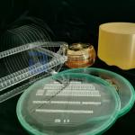
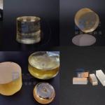
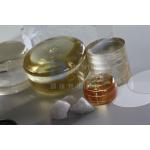
Product Description: Fused Silica Wafer is a kind of Calcium Silicate Board, also known as Glass Wafer. It is a precision engineered and manufactured ...
2024-12-09 22:58:07
|
|
4 inch Diameter LiNbO3 Wafer 0.25mol% Er dope or 5mol% MgO dope for Optical Applications LiNbO3 (LN) crystal has stable physical, chemical and ...
2025-07-30 00:13:57
|
|
4 inch Diameter LiNbO3 Wafer 0.25mol% Er dope or 5mol% MgO dope for Optical Applications LiNbO3 (LN) crystal has stable physical, chemical and ...
2025-07-30 00:13:57
|

|
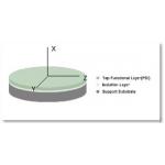
SAW propagation on the Piezoelectric Wafer with Designed Cut Angles and Thickness A piezoelectric material is a crystal that has the ability to ...
2024-12-09 20:34:25
|