
51 - 60 of 75
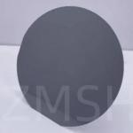
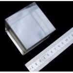
square gallium oxide wafer
Selling leads
|
...Wafer Silicon Carbide Optoelectronic High-Power RF LEDS Description of 3C-N SiC Wafer: Compared to 4H-Sic, although the bandgap of 3C silicon ...
2025-05-06 20:41:48
|
|
10x10mmt Terbium gallium garnet (TGG)crystals substrate wafer for laser device Product Type: Yttrium aluminum garnet (YAG) is an isotropic crystal ...
2025-07-25 00:10:23
|
|
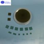
SiO2 wafer Thermal Oxide Laver Thickness 20um+5% MEMS Optical Communication System Product Description: The SIO2 silicon dioxide wafer serves as a ...
2025-05-06 20:45:05
|
|
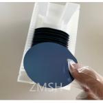
2inch/3inch/4inch/6inch 6H-N/4H-SEMI/ 4H-N SIC ingots/High purity 4H-N 4inch 6inch dia 150mm silicon carbide single crystal (sic) substrates wafers, ...
2025-05-06 20:40:52
|
|
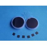
10x10mmt/Tellurium oxide (TeO2) crystals crystal substrate TeO2 wafer TeO2 Crystal & Q Switch TeO2 is an excellent ascousto-optic (AO) crystal with ...
2025-05-06 20:40:28
|
|
MgO Wafer (111) (100) Polished Magnesium oxide Monocrystal Semiconductor Customized *, *::before, *::after {box-sizing: border-box;}* {margin: 0;}html...
2025-05-06 20:45:34
|
|
2-4inch Gallium antimonide GaSb Substrate Single Crystal Monocrystal for Semiconductor InAsSb/In-AsPSb, InNAsSb and other heterojunction materials can ...
2025-05-06 20:44:36
|
|
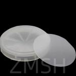
SIC square substrate 5×5 10×10 350um Off axis: 2.0°-4.0°toward Production grade SIC square substrate's abstract Silicon carbide (SiC) square ...
2025-05-06 20:41:37
|
|
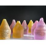
...) for sapphire crystal growth is currently used by many companies in China to produce sapphire for the electronics and optics industries. High...
2025-05-06 20:39:27
|
|
...WAFER WINDOW for OPTICAL LASER OPTICS APPLICATIONS High hardness Ir Optical Standard Window Multiple shapes sapphire window Optical Glass BK7...
2025-07-25 00:10:23
|