
21 - 30 of 75
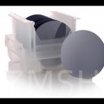
square gallium oxide wafer
Selling leads
|
...) are 3D integrated at the wafer scale. The two wafers are bonded face-to-face using a low-temperature oxide-oxide bonding technique. The Si ...
2025-05-06 20:44:26
|
|
... Wafer Characteristic III-Nitride(GaN,AlN,InN) Gallium Nitride is one kind of wide-gap compound semiconductors. Gallium Nitride (GaN) substrate is ...
2025-05-06 20:44:18
|
|
...Gallium arsenide GaAs Wafer Product Description (GaAs) Gallium Arsenide Wafers PWAM Develops and manufactures compound semiconductor substrates...
2025-05-06 20:44:31
|
|
... (GaAs) Gallium Arsenide Wafers Gallium arsenide (GaAs) is a compound of the elements gallium and arsenic. It is a III-V direct bandgap semiconduct...
2025-05-06 20:44:31
|
|
... (GaAs) Gallium Arsenide Wafers Gallium arsenide (GaAs) is a compound of the elements gallium and arsenic. It is a III-V direct bandgap semiconduct...
2025-05-06 20:44:43
|
|
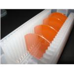
...Gallium phosphide (GaP) crystals crystal substrate,GaP wafer ZMKJ can provides 2inch GaP wafer – gallium Phosphide which are grown by LEC(Liquid ...
2025-05-06 20:44:33
|
|
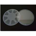
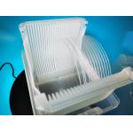
...Wafer SSP DSP Product Description: Sapphire bonding sheet is used for thinning and polishing of gallium arsenide wafers Due to the weight and ...
2025-07-22 00:12:04
|
|
Product Description: Our InP (Indium Phosphide) semiconductor wafers, renowned for their exceptional electronic and optoelectronic properties, have ...
2025-05-06 20:44:23
|
|
Product Description: Our InP (Indium Phosphide) wafers are renowned for their low defect density and high performance, widely used in optoelectronics ...
2025-05-06 20:44:24
|
|
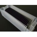
...wafer DSP SiO2 wafers Silicon oxide wafer 1inch 2inch 10x10mm Scanning electron microscope silicon wafer small square piece SEM Polished Silicon ...
2025-05-06 20:44:47
|