
141 - 150 of 175
solar cells silicon wafer
Selling leads
|
...Wafer Semiconductor Substrate For Epitaxial Growth VGF 2inch 4inch 6inch n-type prime grade GaAs wafer for epitaxial growth Gallium arsenide can be ...
2025-05-06 20:45:00
|
|
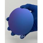
SiO2 wafer Thermal Oxide Laver Thickness 20um+5% MEMS Optical Communication System Product Description: The SIO2 silicon dioxide wafer serves as a ...
2025-05-06 20:45:05
|
|
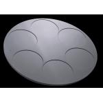
...Silicon Carbide SiC Coated Graphite Tray High Temperature Resistance Graphite Plates Silicon carbide coated epitaxial sheet tray used in epitaxial ...
2025-05-06 20:47:41
|
|
... Formula Al2O3 Crystal Stucture Hexagonal System ((hk o 1) Unit Cell Dimension a=4.758 Å,Å c=12.991 Å, c:a=2.730 PHYSICAL Metric English (Imperial) ...
2025-05-06 20:38:40
|
|
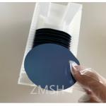
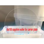
...DSP wafers with 650um/1000um Thickness with notch type for semiconductor carrier plates/sos/ pss/optical About synthetic sapphire crystal Sapphire ...
2025-05-06 20:38:48
|
|
Abstract The 4-H Semi-Insulating SiC substrate is a high-performance semiconductor material with a wide range of applications. It derives its name ...
2025-08-01 00:08:35
|
|
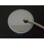
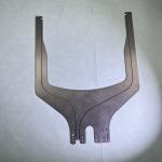
... fork custom-made precision structural component, handle wafers, optical component Abstract of SiC ceramic fork SiC Ceramic Fork Arm is a ...
2025-08-01 00:08:35
|
|
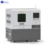
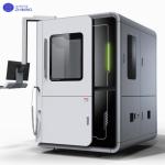
Product Introduction The microjet laser device is a revolutionary precision machining system that achieves thermal damage-free, high-precision ...
2025-05-06 20:43:55
|
|
*, *::before, *::after {box-sizing: border-box;}* {margin: 0;}html, body {height: 100%;}body {line-height: 1.5;-webkit-font-smoothing: antialiased;...
2025-05-06 20:45:05
|
|
Product Introduction Microjet laser technology equipment is a combination of laser and high-speed water jet advanced processing technology, its core ...
2025-05-06 20:43:56
|