
131 - 140 of 169
sio2 silicon dioxide wafer
Selling leads
|
... with notch DSP Sapphire Substrate wafers thickness 1.15mm C-a Sapphire application Application Sapphire wafer and substrate applications include: ...
2025-05-06 20:40:27
|
|
... technology, revolutionizing the landscape of advanced electronics. Comprising three distinct layers, this cutting-edge wafer embodies a trifecta ...
2025-05-06 20:45:07
|
|
4inch 6inch 300-900 nm Lithium Niobate LiNbO3 LN Thin Films (LNOI) on silicon wafer Direction of application: · Electro-Optic Modulators · Delay Lines ...
2025-05-06 20:44:42
|
|
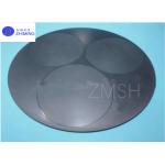
Silicon Carbide Trays SiC wafers tray plate for ICP etching MOCVD Susceptor Wear Resistant Description SIC coated graphite trays are crafted from high ...
2025-08-03 00:08:11
|
|
SiC Ceramic Tray/Plate/Wafer Holder for ICP Etching Process Used in Epitaxial Growth Processing Abstract of SiC (Silicon Carbide) Ceramic Trays ...
2025-05-06 20:47:48
|
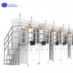
Silicon Carbide Monocrystalline Growth Furnace Resistance Method 6 8 12inch SiC Ingot Growth Furnace
|
... proudly introduces its SiC single crystal growth furnace, an advanced solution engineered for high-performance SiC wafer manufacturing. Our ...
2025-05-06 20:43:51
|
|
... Sapphire based AlN templates AlN film on sapphire substrate sapphire window sapphire wafer Applications of AlN template Silicon-based semiconducto...
2025-05-06 20:44:39
|
|
...WAFER WINDOW for OPTICAL LASER OPTICS APPLICATIONS High hardness Ir Optical Standard Window Multiple shapes sapphire window Optical Glass BK7...
2025-08-03 00:08:11
|
|
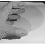
...Wafer Semiconductor Substrate For Epitaxial Growth VGF 2inch 4inch 6inch n-type prime grade GaAs wafer for epitaxial growth Gallium arsenide can be ...
2025-05-06 20:45:00
|
|
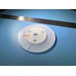
8inch Si Wafer Si Substrate 111 P Type N Type for Micro-electromechanical systems (MEMS) Or Power semiconductor devices Or Optical components and ...
2025-05-06 20:45:50
|