
111 - 120 of 169
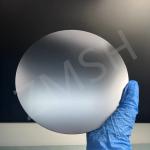
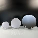
sio2 silicon dioxide wafer
Selling leads
|
... conductivity properties, which can be precisely modified through doping with elements like phosphorus or boron, make them ideal for fabricating ...
2025-05-06 20:45:58
|
|
...Wafers Thickness 0.5mm High Transmittance UV Quartz Glass Sheet 0.2mm--- 1.0mm thickness LED Back Light quartz/borofloat Glass Wafer Polished ...
2025-05-06 20:39:24
|
|
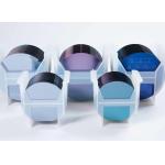
SiC Substrate Silicon carbide subatrte 4H/6H-P 3C-N 5×5 10×10mm P grade R grade D grade 4H/6H-P SiC Substrate 5×5 10×10mm's abstratct The 4H/6H-P ...
2025-05-06 20:41:41
|
|
... Silicon Wafers Ultra-High Purity Optoelectronic-Grade Abstract The high-purity silicon wafer we offer undergoes precision machining and strict ...
2025-05-06 20:45:04
|
|
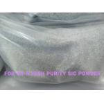
high purity 99.9995% sic powder for 4H-N and un-doped 4h-semi sic crystal growth About Silicon Carbide (SiC)Crystal Application of SiC SiC crystal is ...
2025-05-06 20:40:55
|
|
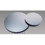
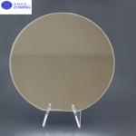
Silicon Wafer CZ orientation111 Resistivity: 1-10 (ohm.cm) single side or double side polish Product abstract Our Si wafer offers high purity and ...
2025-05-06 20:45:12
|
|
...Wafer 6inch 150mm SiC type 4H-N Si type N or P N-type SiC on Si Compound Wafer abstract N-type silicon carbide (SiC) on silicon (Si) compound ...
2025-05-06 20:45:18
|
|
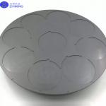
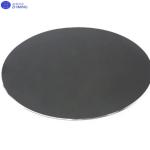
silicon carbide ceramic tray Used to support materials semiconductor wafers Excellent corrosion resistance. silicon carbide ceramic tray‘s short brief ...
2025-05-06 20:47:46
|
|
Silicon wafer Conductivity Solar Cells Solar Cells Power Semiconductor Devices High Purity Product Description: Attributes Details Substrate Material ...
2025-05-06 20:45:09
|
|
...Wafer with (111) Crystal Orientation – Introduction The 8-inch silicon wafer with (111) crystal orientation is a vital component in the semiconduct...
2025-05-06 20:45:52
|