
311 - 320 of 372
single crystal silicon wafers
Selling leads
|
...500–600 nm, depending on specific applications) onto a silicon dioxide (SiO₂) substrate. SiC is renowned for its exceptional thermal conductivity, ...
2025-05-27 17:33:30
|
|
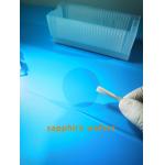
...wafers for GaN epitaxial growth;0.1mm/100um 2inch sapphire c-axis substrates 2Inch 3inch 4inch 0.43mm 0.1mm ultrathin thickness double side polish ...
2025-05-06 20:38:50
|
|
... crystal sapphire, making them ideal for demanding applications (such as laser systems) because of their extreme surface hardness, high thermal ...
2025-05-06 20:42:40
|
|
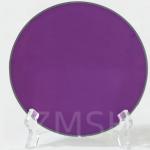
...Wafer Square Rectangle Sapphire Optical Windows , Single Crystal Glass For LED Chip Al2O3 Crystal Materials Step Sapphire Optical Windows With High ...
2025-05-06 20:38:07
|
|
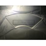
... synthetic Sapphire crystal OEM Size and Design, any shape is ok; Widely used for optical window, lens, military, etc; The material is synthetic ...
2025-05-06 20:39:14
|
|
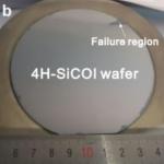
... wafer is a specialized type of wafer that combines the properties of silicon carbide and silicon materials. The wafer consists of a layer of semi...
2025-05-06 20:45:23
|
|
... Extreme Surface Hardness and Chemical Resistance ③- Transmits Wavelengths Ranging From UV to Mid-Infrared Sapphire Windows are manufactured from ...
2025-05-06 20:37:31
|
|
... Extreme Surface Hardness and Chemical Resistance ③- Transmits Wavelengths Ranging From UV to Mid-Infrared Sapphire Windows are manufactured from ...
2025-05-06 20:43:33
|
|
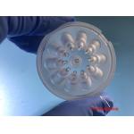
10x10mmt Terbium gallium garnet (TGG)crystals substrate wafer for laser device Product Type: Terbium gallium garnet (TGG) crystal substrateProduct ...
2025-05-06 20:40:28
|
|
... AlN Wafer Characteristic III-Nitride(GaN,AlN,InN) 2inch AlN template on sapphire or sic substrates, HVPE Gallium Nitride wafer,AlN substrates on ...
2025-05-06 20:44:29
|