
281 - 290 of 372
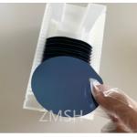
single crystal silicon wafers
Selling leads
|
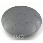
Silicon Carbide Trays SiC wafers tray plate for ICP etching MOCVD Susceptor Wear Resistant Description SIC coated graphite trays are crafted from high ...
2025-07-30 00:08:00
|
|
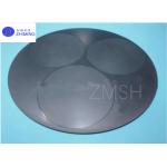
SiC Ceramic Tray/Plate/Wafer Holder for ICP Etching Process Used in Epitaxial Growth Processing Abstract of SiC (Silicon Carbide) Ceramic Trays ...
2025-05-06 20:47:48
|
|
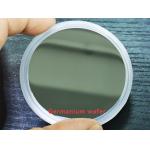
...germanium wafers, which is short for Ge wafers grown by VGF / LEC. Lightly doped P and N-type Germanium wafers can be also used for the Hall effect ...
2025-05-06 20:44:50
|
|
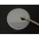
... Sapphire based AlN templates AlN film on sapphire substrate sapphire window sapphire wafer Applications of AlN template Silicon-based semiconducto...
2025-05-06 20:44:39
|
|
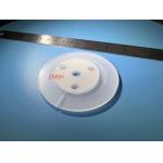
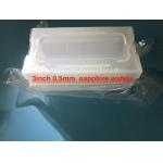
...WAFER WINDOW for OPTICAL LASER OPTICS APPLICATIONS High hardness Ir Optical Standard Window Multiple shapes sapphire window Optical Glass BK7...
2025-07-30 00:08:00
|
|
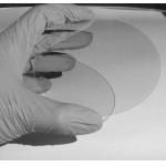
...Wafer Semiconductor Substrate For Epitaxial Growth VGF 2inch 4inch 6inch n-type prime grade GaAs wafer for epitaxial growth Gallium arsenide can be ...
2025-05-06 20:45:00
|
|
SiO2 wafer Thermal Oxide Laver Thickness 20um+5% MEMS Optical Communication System Product Description: The SIO2 silicon dioxide wafer serves as a ...
2025-05-06 20:45:05
|
|
... Formula Al2O3 Crystal Stucture Hexagonal System ((hk o 1) Unit Cell Dimension a=4.758 Å,Å c=12.991 Å, c:a=2.730 PHYSICAL Metric English (Imperial) ...
2025-05-06 20:38:42
|
|
...crystal. It belongs to the cubic crystal system. Nd∶GGG doped with Nd is an excellent laser crystal, which can obtain pulsed laser output at room ...
2025-05-06 20:40:33
|
|
... (20000 photons/MeV) and a rapid light decay time (70ns), making it excel in particle detection. Furthermore, Ce:YAG single crystal exhibits ...
2025-07-30 00:08:00
|