
41 - 50 of 159
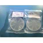
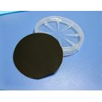
single crystal gallium nitride wafer
Selling leads
|
... of applications. In fact, sapphire is one of the hardest and most scratch-resistant materials available, with a Mohs hardness of 9, second only to ...
2025-08-01 00:08:35
|
|
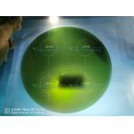
2inch/3inch/4inch/6inch 6H-N/4H-SEMI/ 4H-N SIC ingots/4inch 6inch silicon carbide SIC 4H-N seed crystal Wafer For crystal growth About Silicon Carbide ...
2025-05-06 20:40:48
|
|
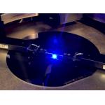
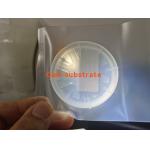
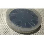
... Wafer Characteristic III-Nitride(GaN,AlN,InN) Gallium Nitride is one kind of wide-gap compound semiconductors. Gallium Nitride (GaN) substrate is ...
2025-05-06 20:44:18
|
|
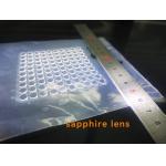
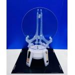
...crystal circle lens,Al2O3 single crystal glass wafer, sapphire lens sapphire optical lens, Al2O3 single crystal glass ,sapphire optical glass ...
2025-05-06 20:37:47
|
|
...wafer for LeD,semiconducting Gallium Nitride Wafer for ld,GaN template, mocvd GaN Wafer,Free-standing GaN Substrates by Customized size,small size ...
2025-05-06 20:44:28
|
|
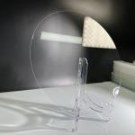
C-axis (0001) orientation 3inch diameter 76.2mm sapphire wafer sapphire glass sapphire watch glass ar sapphire crystal sapphire wafer price 2inch ...
2025-08-01 00:08:35
|
|
...wafer for LeD,semiconducting Gallium Nitride Wafer for ld,GaN template, mocvd GaN Wafer,Free-standing GaN Substrates by Customized size,small size ...
2025-05-06 20:44:12
|
|
...blade for razor,Al2O3 single crystal glass wafer,artificial sapphire injector ,sapphre lenssapphire optical lens, Al2O3 single crystal glass ...
2025-05-06 20:42:29
|
|
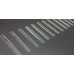
2inch/3inch/4inch S/Fe/Zn doped InP Indium Phosphide Single Crystal Wafer Indium phosphide (InP) is an important compound semiconductor material with ...
2025-05-06 20:44:34
|
|
2inch InP wafers 3inch 4inch N/P TYPE InP Semiconductor Substrate Wafers Doped S+/ Zn+ /Fe + growth (modified VFG method) is used to pull a single ...
2025-05-06 20:44:36
|